Drass wrote:
dr Jefyll's suggestion [...] avoids the partial address being placed in the bus during "dead" cycles.
Uh, nope!
Drass wrote:
All my testing suggests absolute indexed addressing re-reads the PC address during the "dead" cycle if a page is crossed.
Yes.
My suggestion avoids the read-before-write of a fully-formed address. I think that's what you meant but you were just typing too fast. To be clear, "
partial address" refers to the situation where the low byte of an address is valid but the high byte is 1 less than it ought to be. (The high byte needs to be incremented because addition performed on the low byte has produced a carry. IOW a page-crossing has occurred.)
AFAIK the 'C02
never places a partial address on the bus -- I believe they *did* entirely eliminate that particular misbehavior.
In every case where the NMOS chip would've produced a partial address, the CMOS chip will place PC on the bus instead -- I've seen no evidence to contradict this. But this doesn't cover the situation mentioned upthread, namely an indexed STA
without a page crossing. An NMOS chip will immediately present the complete address, first reading from it then writing to it.

And Drass discovered the CMOS chip does the same! My suggestion avoids this because it ensures a page crossing. So, we get a read via PC then a write to the fully-formed address.
Drass wrote:
I was thinking about using RDY to implement the wait-state circuit for Rev 2 of the SBC. Since I have Rev 1 to use for debugging the TTL CPU, Rev 2 can dispense with a lot of complexities and just focus on speed
Hey, wait a minute! Recently you said you were resisting the urge to develop new software because it would distract you from the main project -- the TTL 6502. But now you're getting distracted with new hardware!?

Drass wrote:
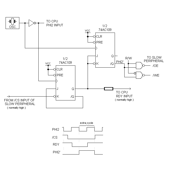
I'm thinking the solution is to derive /OE and /WE from PHI2', where PHI2' = (PHI2 OR /RDY). That should keep the read and write enable signals low for the extra cycle and give peripherals enough time to respond.
I like the PHI2' idea but I'd generate it differently. If I understand correctly your method gives OE and WE pulses which endure for 1.5 cycles -- they begin very soon during the 2-cycle period devoted to the access. It'd be better to increase the address setup time seen by the peripheral by having the OE and WE pulses endure for only half of the 2-cycle period.
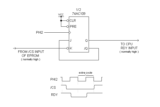
Posted below are the original wait-state circuit discussed
elsewhere and a revised version with added logic to generate PHI2'. Extra sets of eyes welcome -- I'm up past my bedtime!
BigDumbDinosaur wrote:
your logic has to know whether RDY is low because of a wait-state or because of a WAI instruction.
Darn! -- I overlooked that. But after blinking my eyes for a while I concluded you must be getting sleepy, too, BDD. The logic we're talking about is in charge of generating OE and WE for the slow peripheral. And WAI doesn't address the slow peripheral. WAI's bus activity only involves code memory.
However, you're right about RDY being bidirectional, which means a resistor as shown may be desirable to limit current flow. Details of this are hashed over in the post I linked to.

-- Jeff
Attachment:
 simple wait-state generator.gif [ 4 KiB | Viewed 1034 times ]
Attachment:
 wait-state generator with OE + WE.png [ 8.2 KiB | Viewed 1034 times ]


