16a) T1H //Timer 1 high (Bit 8..15)
Timer 1 is a down counter, counting at PHI2 speed.
Down counter means:
If the carry input of a counter cell is active, the counter will toggle in the pending clock phase.
If the carry input of a counter cell is active and the counter Bit is 0,
the output carry goes active.
Conceptually, it's very similar to what we had in "15c) T2H",
except that the latches can be read back to the data bus.
Counter cells have a fully transparent static latch,
High_active control signal W_T1H_latch loads the latches from the write data bus during PHI0=0.
High_active control signal T1H_LD transfers the write data bus into the counter Bits.
High_active control signal T1H_CNT tranfers "the new counter value" into the counter Bits.
One of these two signals are active when PHI0=0 AND PHI2=0,
and they are generated in "16b) T1H control".
High_active control signal R_T1H reads the T1H counter Bits into the read data bus.
High active control signal R_T1H_latch reads the T1H latch back into the read data bus.
One of these two signals can be active when PHI1=0 (what is different from PHI2=1).
Counter Bits 8,10,12,14 have low_active input carry and high_active output carry,
Counter Bits 9,11,13,15 have high_active input carry and low_active output carrry.
T1H_cin8# is the low_active carry input of the T1H Bit 8 counter cell,
and it's just generated from the high_active T1L_TC signal by using an inverter.
The five counter Bits 8..12 are linked together by ripple carry.
A NOR gate checks if the Bits 8..12 are 0, and if T1H_cin8# is active.
It then generates the high_active T1_TC signal, what is the input carry
for counter Bit 13.
The three counter Bits 13..15 are linked together by ripple carry again.
Attachment:
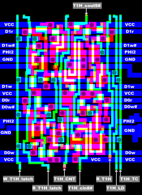 si6522_16a_t1h.png [ 42.66 KiB | Viewed 1057 times ]
;---
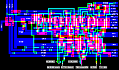
16b) T1H control
It is based on the circuitry we already had in "15d) T2H control".
We have a RS flipflop, which is set when T1H counter is written with W_T1HC
Note:
Writing to $7 T1H latch does not set the RS flipflop or write T1H counter.
Writing to $5 T1H counter does set the RS flipflop and writes T1H latch.
When T1H is not written AND there is a Timer 1 underflow (indicated by T1H Bit 15 output carry)
AND the RS flipflop is set (sampled by a transparent latch during PHI1=1),
this will set IFR6 (Timer 1 interrupt flag) during PHI2=1,
and if Timer 1 is running one_shot (ACR6=0) this clears the RS flipflop during the next PHI1=1.
If Timer 1 is running continous interrupts (ACR6=1), the RS flipflop is not cleared.
Note: when the RS flipflop is cleared, Timer 1 still will count,
and Timer 1 still will be reloaded from the Timer 1 latches after there was a Timer 1 underflow.
Also, T1H control generates two high_active control signals of which only one is active
during PHI0 AND PHI2: T1H_LD and T1H_CNT (these signals already went described above in the text).
And it generates the high_active T1_LD signal, which goes into "16d) T1L control",
indicating a Timer 1 load.
PB7_T1 is the signal which goes into the PB7 output driver when Timer 1 emits a pulse
or a square wave on PB7. //In this case, PB7 = PB7_T1.
It is generated by a toggle flipflop, which is cleared runing a T1H counter write,
set when ACR7=0 (when Timer 1 does not use PB7),
and it toggles during PHI2 after a Timer 1 underflow when the "Timer 1 active" RS flipflop is set.
;
Note, that for the toggle flipflop, clear has highest priority, and toggle has lowest priority.
Attachment:
 si6522_16b_t1h_ctrl.png [ 58.12 KiB | Viewed 1057 times ]
;---
16c) T1L //Timer 1 low (Bit 7..0)
Timer 1 always is running at PHI2 speed, and that's why counter Bit 0 has no input carry:
Bit 0 just always toggles at PHI2 speed, and it has a high_active output carry.
Timer 1 is a down counter using an inverting/non_inverting carry chain. //ripple carry.
Counter Bits 2,4,6 have low_active input carry and high_active output carry,
Counter Bits 1,3,5,7 have high_active input carry and low_active output carrry.
Counter cells have a fully transparent static latch,
High_active control signal W_T1L_latch loads the latches from the write data bus during PHI0=0.
High_active control signal T1L_LD transfers the write data bus into the counter Bits.
High_active control signal T1L_CNT tranfers "the new counter value" into the counter Bits.
One of these two signals are active when PHI0=0 AND PHI2=0,
and they are generated in "16d) T1L control".
High_active control signal R_T1L reads the T1L counter Bits into the read data bus.
High active control signal R_T1L_latch reads the T1L latch back into the read data bus.
One of these two signals can be active when PHI1=0 (what is different from PHI2=1).
High_active signal T1L_TC indicates a Timer 1 low terminal count,
means that T1L_TC is high if T1L=$00,
what will make the T1L down counter Bits roll over to $FF during PHI0=0 AND PHI2=0.
Note, that T1L_TC changes during PHI2=1.
;
Of course, in the silicon the NOR gate is broken into 8 parts,
attached to each of the counter Bits, to make better use of chip space.
Attachment:
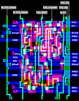 si6522_16c_t1l.png [ 45.47 KiB | Viewed 1057 times ]
;---
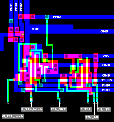
16d) T1L control
T1_LD generated in "16b) T1H control" indicates a Timer 1 load.
From this signal, T1L control generates the two control signals
T1_LD and T1L_ CNT. That's all there is to it.
Attachment:
 si6522_16d_t1l_ctrl.png [ 26.35 KiB | Viewed 1057 times ]
;===
Attachment:
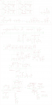 6522_16_timer1.png [ 291.41 KiB | Viewed 1057 times ]


