Quote:
Quote:
Quote:
but the state of /OE should be qualified by R/W
The SRAM's data pins are always in input mode if R/W\ is low though.
In theory. However, different manufacturers may implement their control logic in subtly different ways. I prefer to assume the worse in that regard.
I've found minor differences in 6522's and 4094's made by different manufacturers, so it's always good to watch for that. But I've looked at a lot of RAM data sheets over the years, and they have been 100% consistent in that they will never enable their outputs when you're trying to write to them.
Quote:
Quote:
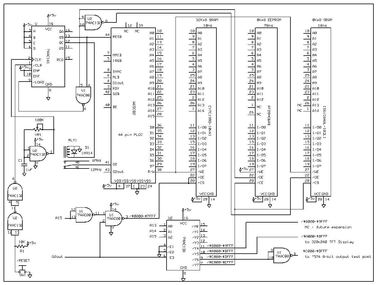
He has φ2 brought into the RAM selects, so he's in good shape there.
As far as avoiding inadvertent writes, that would be correct. However, doing so has the effect of delaying the RAM select until Ø2 goes high, which would limit the maximum speed at which the circuit would run.
He has two gate delays in the path to /CS and /OE. U1's output won't go low until Ø2 is high, so that's 6-10 NS right there into the time when D0-D7 is valid. Plus there's the 6-10 NS of U4 following A15 changing state. I'd scrap the Ø2 qualification of the SRAM select, instead use Ø2 to qualify R/W and hook A15 directly to the SRAM's /CS. SRAM is going to be in anytime the address is less than $8000, so no need for any additional logic in that department. With A15 directly driving /CS, he'd have almost all of Ø2 low to get the address setup done. As soon as Ø2 went high, the SRAM would be ready for read/write. Just an opinion, of course.
You're driving me back to the timing diagrams again, which is good. It may affect how I work my next workbench computer's logic. In the 14MHz 65c02, the address set-up time is not guaranteed to be less than 30ns. A half cyle at 14MHz is 35.7ns, so there's less than 6ns improvement there over when φ2 rises. We all know however that the specs are extreme conservative, so there's probably more time available there, depending on the clock speed. Electric_Eye does have the other RAM on the right for the OS and vectors through the '138 which has a lot more delay.
Electric_Eye, this does bring up something I didn't catch before. You have $8000-$9FFF set out there for future expansion; but if you ever decide to put a 65c22 out there, that enable cannot be gated by φ2. That I/O IC and others in the 65 family need the selects to be true
before φ2 rises, or they won't work.
Quote:
I see a few other problems lurking with your push button circuits. Pressing S1 has the effect of shorting both C1 and C2 to ground, producing a high momentary current flow that will eventually cause the push button's contacts to stick together.
I would put a resistor in series to limit the current to a milliamp or so. The bigger threat is usually when a switch is opened, because of arcking which burns the contacts, little by little. It's worst if you have an inductive load (which is not the case here) and no diode across the switch to protect it from the voltage spike when you open the contacts. The amount of energy in a 1µF capacitor won't melt and weld those contacts though.
Quote:
Also, the values for R1 and R2 are much too high. I know you are trying to avoid the use of large capacitors to achieve a desired time-constant. The problem with doing so is the effects of capacitor leakage on the final voltage once they've charged.
The resistor values might be a little high, but I would mainly reduce them so that the CMOS input leakage doesn't compete with the resistors' current. The CMOS input leakage is not guaranteed to be less than a couple of µA. That's more than the capacitors will leak. My designs are in a lot of aircraft and do this kind of thing with never a problem except the rare case where a capacitor is internally shorted (not just leaky) or the capacitor is making a lot of noise as a result of leakage that's too small to upset the bias. That's pretty rare though, after putting millions of capacitors in the field in our products. I'm the only one who fixes our stuff, so I know what the failures are (which BTW have been extremely few, and most are infant mortality-- IOW, if something makes it through the first few months without problems, it probably will
never have problems.) And after my comment about the specified tolerances of electrolytic capacitors, I remembered a timer circuit that's in half of our aircraft intercoms that uses a time constant of 20 seconds, and we never had a problem with the timing being wrong because of slight leakage or even the electrolytics' supposed tolerance. (It wouldn't matter if it's a few seconds one way or the other, but it has been quite consistent.) It's one of those things where you do something the spec.s or urban legend say you can't, but you find out from observation and experimentation that you can, and then you forget about it because that part never gave a single problem in over 20 years.
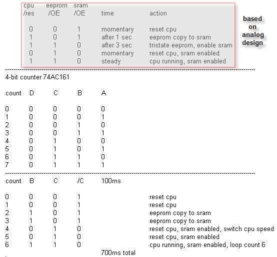
Electric_Eye, how do you plan to change the clock frequency to a higher one after pre-loading the RAM?
Quote:
...And the CPU needs to be reset the second time because the reset vector will be modifed before the 2nd reset so after the second reset the OS will start above the piece of software that copies the OS to itself, or else there would be an endless loop.
Just copy the OS to itself then JMP to wherever the second reset routine is. That way it won't require any hardware tricks (except that one way or another, you do still need to kick the clock speed up, to accomplish the purpose).
Quote:
I don't know what will happen when the switch from EEPROM to SRAM
actually occurs, since the switching is not clocked (won't cause any
problems is my guess)
If the clock frequency is switched while the processor is running, you'll definitely need to take measures to prevent glitches. If switching clock sources results in the φ0 input clock getting a one-time pulse that's less than the minimum width the system will work with (say 25ns or so) the computer will crash. A "runt pulse" would be when the pulse is so short it doesn't even quite have time to fully get to the oposite logic state and back. That would sometimes cause crashes too.
What I'm tentatively planning to do is to use a PIC microcontroller to copy the OS from an 8-pin plug-in serial EEPROM to the SRAM before it releases the microprocessor and gets out of the way. If I develop it for myself then I don't mind making it available for others too, although you probably don't want to wait for me. I don't do anything quickly.