6502.org Forum  Projects  Code  Documents  Tools  Forum
It is currently Mon Nov 04, 2024 9:04 pm

All times are UTC


Post new topic Reply to topic  [ 103 posts ]  Go to page Previous  1, 2, 3, 4, 5 ... 7  Next
Author Message
 Post subject:
PostPosted: Sun Jan 03, 2010 8:42 pm 
Offline

Joined: Mon Mar 02, 2009 7:27 pm
Posts: 3258
Location: NC, USA
BigDumbDinosaur wrote:
... That said, why not arrange your address decoder to simply map out the EPROM after transferring it to SRAM instead of reseting the circuit twice?


I am "mapping out" the EEPROM by disabling the /OE, and enabling the /OE on the SRAM. Am I missing something here? You are not the only one to say this BDD.

With the SRAM "shadowed" underneath the EEPROM, everytime the EEPROM writes to itself, it is actually writing to the SRAM.

...And the CPU needs to be reset the second time because the reset vector will be modifed before the 2nd reset so after the second reset the OS will start above the piece of software that copies the OS to itself, or else there would be an endless loop.

_________________
65Org16:https://github.com/ElEctric-EyE/verilog-6502


Top
 Profile  
Reply with quote  
 Post subject:
PostPosted: Sun Jan 03, 2010 11:13 pm 
Offline
User avatar

Joined: Thu May 28, 2009 9:46 pm
Posts: 8474
Location: Midwestern USA
ElEctric_EyE wrote:
With the SRAM "shadowed" underneath the EEPROM, everytime the EEPROM writes to itself, it is actually writing to the SRAM.

I'm having a little troubled determining how that would be the case. Part of it is the image in your first post is a bit difficult to read. The small print that indicates what gets mapped to where is a little smaller than my weak vision can handle. So I might be missing something.

_________________
x86?  We ain't got no x86.  We don't NEED no stinking x86!


Top
 Profile  
Reply with quote  
 Post subject:
PostPosted: Sun Jan 03, 2010 11:18 pm 
Offline
User avatar

Joined: Thu May 28, 2009 9:46 pm
Posts: 8474
Location: Midwestern USA
ElEctric_EyE wrote:
I went out of my budget to order some other IC's too like some 10ns 32Kx8, and 10ns 8Kx8 SRAMs, even though they're SOJ packages.

I built up my POC using SOJ SRAM. It wasn't too tough to mount it. Just don't try to solder those dinky little pins with a lot of caffeine in your system. :)

Quote:
Had to spend an extra $40 to get the 28pin SOJ to 28pin 300mil PDIP @ $7 a pop...

You going to wirewrap this thing?

_________________
x86?  We ain't got no x86.  We don't NEED no stinking x86!


Top
 Profile  
Reply with quote  
 Post subject:
PostPosted: Sun Jan 03, 2010 11:27 pm 
Offline

Joined: Mon Mar 02, 2009 7:27 pm
Posts: 3258
Location: NC, USA
Yes, with the 300mil 28pin SOJ to 28pin PDIP adapter, I intend wirewrapping the "shadowRAM" scheme. If it works, it will be the last chapter before I start designing boards using expressPCB software.

_________________
65Org16:https://github.com/ElEctric-EyE/verilog-6502


Top
 Profile  
Reply with quote  
 Post subject:
PostPosted: Mon Jan 04, 2010 2:08 am 
Offline

Joined: Tue Nov 18, 2003 8:41 pm
Posts: 250
I'm not at all certain I understand what you're trying to do here.
You don't show any circuitry to switch EEPROM/SRAM speeds.
I don't really see what the switches are about.

Assuming you want a power on reset that mirrors EEPROM to SRAM
and a "warm" reset that is initiated manuall by a switch but doesn't copy
EEPROM to SRAM (because that was presumably already done at power
on)

And assuming you're not going to write protect SRAM once it's
written (since you don't show that).

Why not OR two reset sources, one that does the power on/copy timing
stuff and one that just debounces the switch.

Have your reset code attempt to write to an EEPROM/SRAM address.

If it can write an EEPROM/SRAM address, it skips the copying.

If it can't write an EEPROM/SRAM address it does the copy and then
waits until it can write to an EEPROM/SRAM address.

I don't know what will happen when the switch from EEPROM to SRAM
actually occurs, since the switching is not clocked (won't cause any
problems is my guess) but you might want to get several successful
write-read attempts as a sort of debounce/deglitch.

Presumably you will have to clock the switching between EEPROM/
SRAM access speeds any way though.


Personally I think I'd add an IO bit that did the switching and put it
under software control.

I'd also look at the possibility of making a read of EEPROM also be
a write of SRAM (but making that work might be more complicated
than it's worth)


Top
 Profile  
Reply with quote  
 Post subject:
PostPosted: Mon Jan 04, 2010 2:42 am 
Offline

Joined: Mon Mar 02, 2009 7:27 pm
Posts: 3258
Location: NC, USA
Heh, what I am trying to do here is what the thread title says: Increase the speed of the WDC65C02... SRAM access times are much faster than EEPROM access times.

It's an order of magnitude approaching 700%. The SRAM I have on order is 10ns. The EEPROM I am currently using is 70ns. If I can transfer the OS from the EEPROM to the SRAM... It should be a no-brainer, but I'll have to wait till the packages arrive and then experiment.

_________________
65Org16:https://github.com/ElEctric-EyE/verilog-6502


Top
 Profile  
Reply with quote  
 Post subject:
PostPosted: Mon Jan 04, 2010 4:47 am 
Online
User avatar

Joined: Fri Aug 30, 2002 1:09 am
Posts: 8536
Location: Southern California
Quote:
Quote:
Quote:
but the state of /OE should be qualified by R/W

The SRAM's data pins are always in input mode if R/W\ is low though.

In theory. However, different manufacturers may implement their control logic in subtly different ways. I prefer to assume the worse in that regard.

I've found minor differences in 6522's and 4094's made by different manufacturers, so it's always good to watch for that. But I've looked at a lot of RAM data sheets over the years, and they have been 100% consistent in that they will never enable their outputs when you're trying to write to them.

Quote:
Quote:
He has φ2 brought into the RAM selects, so he's in good shape there.

As far as avoiding inadvertent writes, that would be correct. However, doing so has the effect of delaying the RAM select until Ø2 goes high, which would limit the maximum speed at which the circuit would run.

He has two gate delays in the path to /CS and /OE. U1's output won't go low until Ø2 is high, so that's 6-10 NS right there into the time when D0-D7 is valid. Plus there's the 6-10 NS of U4 following A15 changing state. I'd scrap the Ø2 qualification of the SRAM select, instead use Ø2 to qualify R/W and hook A15 directly to the SRAM's /CS. SRAM is going to be in anytime the address is less than $8000, so no need for any additional logic in that department. With A15 directly driving /CS, he'd have almost all of Ø2 low to get the address setup done. As soon as Ø2 went high, the SRAM would be ready for read/write. Just an opinion, of course.

You're driving me back to the timing diagrams again, which is good. It may affect how I work my next workbench computer's logic. In the 14MHz 65c02, the address set-up time is not guaranteed to be less than 30ns. A half cyle at 14MHz is 35.7ns, so there's less than 6ns improvement there over when φ2 rises. We all know however that the specs are extreme conservative, so there's probably more time available there, depending on the clock speed. Electric_Eye does have the other RAM on the right for the OS and vectors through the '138 which has a lot more delay.

Electric_Eye, this does bring up something I didn't catch before. You have $8000-$9FFF set out there for future expansion; but if you ever decide to put a 65c22 out there, that enable cannot be gated by φ2. That I/O IC and others in the 65 family need the selects to be true before φ2 rises, or they won't work.

Quote:
I see a few other problems lurking with your push button circuits. Pressing S1 has the effect of shorting both C1 and C2 to ground, producing a high momentary current flow that will eventually cause the push button's contacts to stick together.

I would put a resistor in series to limit the current to a milliamp or so. The bigger threat is usually when a switch is opened, because of arcking which burns the contacts, little by little. It's worst if you have an inductive load (which is not the case here) and no diode across the switch to protect it from the voltage spike when you open the contacts. The amount of energy in a 1µF capacitor won't melt and weld those contacts though.

Quote:
Also, the values for R1 and R2 are much too high. I know you are trying to avoid the use of large capacitors to achieve a desired time-constant. The problem with doing so is the effects of capacitor leakage on the final voltage once they've charged.

The resistor values might be a little high, but I would mainly reduce them so that the CMOS input leakage doesn't compete with the resistors' current. The CMOS input leakage is not guaranteed to be less than a couple of µA. That's more than the capacitors will leak. My designs are in a lot of aircraft and do this kind of thing with never a problem except the rare case where a capacitor is internally shorted (not just leaky) or the capacitor is making a lot of noise as a result of leakage that's too small to upset the bias. That's pretty rare though, after putting millions of capacitors in the field in our products. I'm the only one who fixes our stuff, so I know what the failures are (which BTW have been extremely few, and most are infant mortality-- IOW, if something makes it through the first few months without problems, it probably will never have problems.) And after my comment about the specified tolerances of electrolytic capacitors, I remembered a timer circuit that's in half of our aircraft intercoms that uses a time constant of 20 seconds, and we never had a problem with the timing being wrong because of slight leakage or even the electrolytics' supposed tolerance. (It wouldn't matter if it's a few seconds one way or the other, but it has been quite consistent.) It's one of those things where you do something the spec.s or urban legend say you can't, but you find out from observation and experimentation that you can, and then you forget about it because that part never gave a single problem in over 20 years.

Electric_Eye, how do you plan to change the clock frequency to a higher one after pre-loading the RAM?

Quote:
...And the CPU needs to be reset the second time because the reset vector will be modifed before the 2nd reset so after the second reset the OS will start above the piece of software that copies the OS to itself, or else there would be an endless loop.

Just copy the OS to itself then JMP to wherever the second reset routine is. That way it won't require any hardware tricks (except that one way or another, you do still need to kick the clock speed up, to accomplish the purpose).

Quote:
I don't know what will happen when the switch from EEPROM to SRAM
actually occurs, since the switching is not clocked (won't cause any
problems is my guess)

If the clock frequency is switched while the processor is running, you'll definitely need to take measures to prevent glitches. If switching clock sources results in the φ0 input clock getting a one-time pulse that's less than the minimum width the system will work with (say 25ns or so) the computer will crash. A "runt pulse" would be when the pulse is so short it doesn't even quite have time to fully get to the oposite logic state and back. That would sometimes cause crashes too.

What I'm tentatively planning to do is to use a PIC microcontroller to copy the OS from an 8-pin plug-in serial EEPROM to the SRAM before it releases the microprocessor and gets out of the way. If I develop it for myself then I don't mind making it available for others too, although you probably don't want to wait for me. I don't do anything quickly.
Top
 Profile  
Reply with quote  
 Post subject:
PostPosted: Mon Jan 04, 2010 6:34 am 
Offline

Joined: Tue Nov 18, 2003 8:41 pm
Posts: 250
GARTHWILSON wrote:

Quote:
I don't know what will happen when the switch from EEPROM to SRAM
actually occurs, since the switching is not clocked (won't cause any
problems is my guess)

If the clock frequency is switched while the processor is running, you'll definitely need to take measures to prevent glitches. If switching clock sources results in the φ0 input clock getting a one-time pulse that's less than the minimum width the system will work with (say 25ns or so) the computer will crash. A "runt pulse" would be when the pulse is so short it doesn't even quite have time to fully get to the oposite logic state and back. That would sometimes cause crashes too.


I wasn't very clear there.

I meant that for what he shows, ie just switching /OE between the
EEPROM and the SRAM after the EEPROM is copied, I wouldn't expect
much of a problem.

But what ever does the actual speed switching would presumably be
synced to the clock in some way.

Since he doesn't show what he means to do I can only guess that
he intends to do another reset and switch the clock during the second reset.


Top
 Profile  
Reply with quote  
 Post subject:
PostPosted: Mon Jan 04, 2010 12:58 pm 
Offline

Joined: Mon Mar 02, 2009 7:27 pm
Posts: 3258
Location: NC, USA
GARTHWILSON wrote:
...Electric_Eye, how do you plan to change the clock frequency to a higher one after pre-loading the RAM?...


I was planning on using a '157 mutiplexer, but I see Digi-Key has all there multiplexers as non-stocked :(. Looking at a SPDT Reed relay, while they are expensive at $10 each, the coil only needs 10mA.


bogax wrote:
...Since he doesn't show what he means to do I can only guess that
he intends to do another reset and switch the clock during the second reset.


That's exactly right. I'll have an updated schematic here very soon...

_________________
65Org16:https://github.com/ElEctric-EyE/verilog-6502


Top
 Profile  
Reply with quote  
 Post subject: Updated schematic
PostPosted: Mon Jan 04, 2010 2:25 pm 
Offline

Joined: Mon Mar 02, 2009 7:27 pm
Posts: 3258
Location: NC, USA
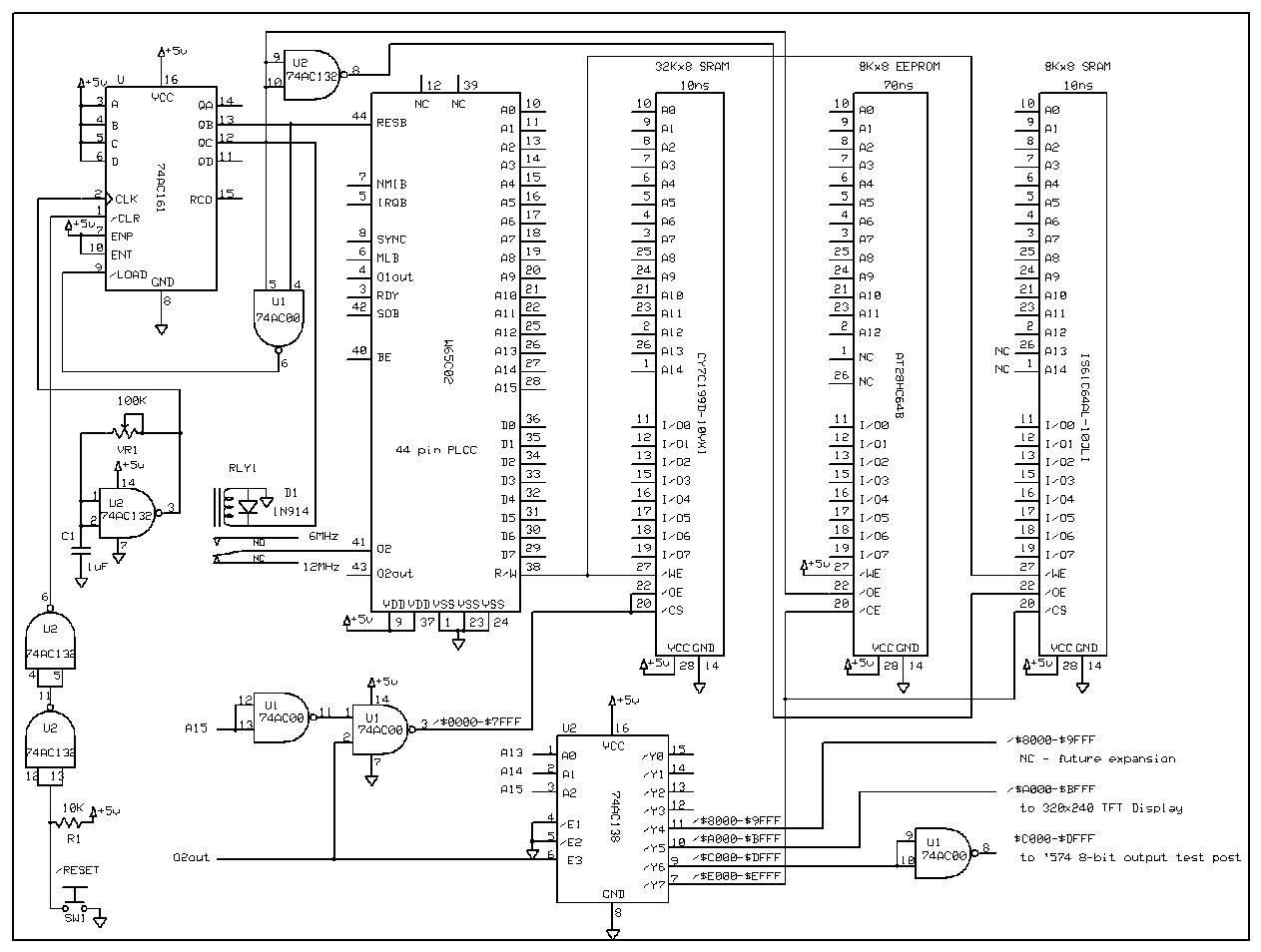
Image
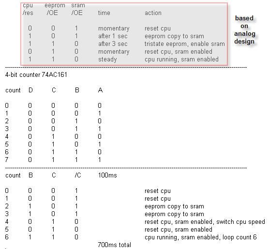
Here's the truth table:

Image

Looking at the schematic again, I realize I can use 1 74AC14 for the 6 inverter functions, and 1 74AC00, and have 2 NAND gates left over. I don't think that the fact they're schmitt triggers will affect anything negatively.

BTW. I did see another 10mA Reed relay for $6... I think it's all going to happen faster than 700mS, which is why I have that trimpot on the oscillator.

Latest edit: I forgot the pull-up resistor for the reset button.

_________________
65Org16:https://github.com/ElEctric-EyE/verilog-6502


Last edited by ElEctric_EyE on Mon Jan 04, 2010 10:13 pm, edited 4 times in total.

Top
 Profile  
Reply with quote  
 Post subject:
PostPosted: Mon Jan 04, 2010 2:35 pm 
Offline

Joined: Mon Mar 02, 2009 7:27 pm
Posts: 3258
Location: NC, USA
BigDumbDinosaur wrote:
... instead use Ø2 to qualify R/W and hook A15 directly to the SRAM's /CS. SRAM is going to be in anytime the address is less than $8000, so no need for any additional logic in that department. With A15 directly driving /CS, he'd have almost all of Ø2 low to get the address setup done. As soon as Ø2 went high, the SRAM would be ready for read/write. Just an opinion, of course.


Would this really work? I've never used phase2 together with R/W to get a good address decode signal.

_________________
65Org16:https://github.com/ElEctric-EyE/verilog-6502


Top
 Profile  
Reply with quote  
 Post subject:
PostPosted: Mon Jan 04, 2010 4:14 pm 
Offline

Joined: Fri Aug 30, 2002 2:05 pm
Posts: 347
Location: UK
Quote:
I was planning on using a '157 mutiplexer, but I see Digi-Key has all there multiplexers as non-stocked . Looking at a SPDT Reed relay, while they are expensive at $10 each, the coil only needs 10mA.

You can use a single 74xx00 to select between the two clock sources.

Lee.


Top
 Profile  
Reply with quote  
 Post subject:
PostPosted: Mon Jan 04, 2010 5:46 pm 
Offline

Joined: Mon Mar 02, 2009 7:27 pm
Posts: 3258
Location: NC, USA
leeeeee wrote:
You can use a single 74xx00 to select between the two clock sources.

Lee.


How?

_________________
65Org16:https://github.com/ElEctric-EyE/verilog-6502


Top
 Profile  
Reply with quote  
 Post subject:
PostPosted: Mon Jan 04, 2010 8:39 pm 
Offline

Joined: Fri Jun 27, 2003 8:12 am
Posts: 618
Location: Meadowbrook
clock hi in 1
2 from 9 and 10 clock control
3 to 13

clock lo in 4
5 from 8 /clock control
6 to 12

13 from 3
12 from 6
11 to clock in of 65c02

10 clock control and to 2
9 clock control and to 2
8 /clock conctrol and to 5


hope that helps. tis basically a single 157 element....

_________________
"My biggest dream in life? Building black plywood Habitrails"


Top
 Profile  
Reply with quote  
 Post subject:
PostPosted: Mon Jan 04, 2010 9:10 pm 
Online
User avatar

Joined: Fri Aug 30, 2002 1:09 am
Posts: 8536
Location: Southern California
Quote:
How?

Tony posted while I was drawing it up an idea. It looks like he has almost exactly what I had, even using the same 74x00 sections, except that there are a couple of things on his where I'm not sure I understand him right. Here's what I got:

CLK0 input to pin 1
CLK1 input to pin 5

SEL input to pins 9 and 4, and pin 10 to Vcc so the 8-9-10 section acts like an inverter.

pin 8 (an output) to pin 2 (an input)

pin 3 (an output) to pin 13 (an input), and
pin 6 (an output) to pin 12 (an input)

Selected clock comes on out pin 11. If SEL=0, you get CLK0 at the output, delayed by two gate delays. If SEL=1, you get CLK1 at the output, again delayed by two gate delays.

There might be a more slick way to do it that I haven't thought of so far. This one can still produce glitches, although that won't matter if you only switch the frequency when RST\ is low.


Top
 Profile  
Reply with quote  
Display posts from previous:  Sort by  
Post new topic Reply to topic  [ 103 posts ]  Go to page Previous  1, 2, 3, 4, 5 ... 7  Next

All times are UTC


Who is online

Users browsing this forum: ojanhk and 6 guests


You cannot post new topics in this forum
You cannot reply to topics in this forum
You cannot edit your posts in this forum
You cannot delete your posts in this forum
You cannot post attachments in this forum

Search for:
Jump to: