6502.org Forum  Projects  Code  Documents  Tools  Forum
It is currently Tue Sep 17, 2024 3:18 am

All times are UTC


Post new topic Reply to topic  [ 135 posts ]  Go to page Previous  1 ... 5, 6, 7, 8, 9
Author Message
 Post subject: Re: Star Ground
PostPosted: Thu Dec 31, 2015 5:02 am 
Offline
User avatar

Joined: Thu May 28, 2009 9:46 pm
Posts: 8382
Location: Midwestern USA
banedon wrote:
It is possible that the GAL is the cause, but I suspect the Winbond W27C512 ROM more as it's the next slowest device and at 45ns (22MHz) is skirting the edge. As Garth says, the speed rating doesn't include set up times, etc., so it's very possible that this is the culprit.

Like Jeff, I think it's your ROM that is the bottleneck. Most GALs are either 10 or 15ns, which is more than sufficient for 20 MHz operation.

You have to consider that a read access on the ROM can only occur during the Ø2 high part of the machine cycle. At 16 MHz, a half cycle would be approximately 31ns. If your ROM were capable only of 45ns access time it would never respond. It just so happens that most devices are able to perform better than advertised due to margins the manufacturers design in to assure their product will meet guaranteed specs when operated at rated voltage and temperature range. You might find that at 16 MHz, a nominal increase in device temperature may cause the circuit to go dead.

For example, I have my POC unit running at 12.5 MHz. This is with a 55ns EPROM. Obviously, I am violating the EPROM's timing, as the half cycle time is 40ns, and access can only occur during Ø2 high. If I increase Ø2 to 15 MHz, the unit might boot or it might not. It all depends on which EPROM I happen to be using at the time, as they vary from part to part, even though they are all the same brand (AMD).

You should see if you can rig up Jeff's wait-state circuit. That will definitively settle the speed issue.

_________________
x86?  We ain't got no x86.  We don't NEED no stinking x86!


Top
 Profile  
Reply with quote  
 Post subject: Re: Star Ground
PostPosted: Thu Dec 31, 2015 8:52 am 
Offline
User avatar

Joined: Sun Sep 08, 2013 10:24 am
Posts: 740
Location: A missile silo somewhere under southern England
One thing: I don't currently qualify reads to the EEPROM with Ø2 and it all seems to work. Is this something that I should be doing? I thought this was only for RAM writes to stop the possibility of rubbish being written.

With regard to Jeff's wait state circuit: I think I might give this a go, but with an added extra: As part of the initialisation routine it would copy itself to the same location in RAM, then switch itself out. So at this point the system can go at full speed with the GAL not allowing writes to that part of the RAM there-after.


Top
 Profile  
Reply with quote  
 Post subject: Re: Star Ground
PostPosted: Thu Dec 31, 2015 9:16 am 
Offline
User avatar

Joined: Fri Aug 30, 2002 1:09 am
Posts: 8508
Location: Southern California
banedon wrote:
One thing: I don't currently qualify reads to the EEPROM with Ø2 and it all seems to work. Is this something that I should be doing? I thought this was only for RAM writes to stop the possibility of rubbish being written.

With the '02, you'll be fine. It's just that with the '816, you need to make sure you take measures to avoid bus contention, as the '816 puts the address high byte out on the data bus during the phase-2-low time, so you wouldn't want the EEPROM to also be putting data out in a way that could make the '816 and the EEPROM fight each other.

_________________
http://WilsonMinesCo.com/ lots of 6502 resources
The "second front page" is http://wilsonminesco.com/links.html .
What's an additional VIA among friends, anyhow?


Top
 Profile  
Reply with quote  
 Post subject: Re: Star Ground
PostPosted: Thu Dec 31, 2015 3:15 pm 
Offline
User avatar

Joined: Thu May 28, 2009 9:46 pm
Posts: 8382
Location: Midwestern USA
banedon wrote:
One thing: I don't currently qualify reads to the EEPROM with Ø2 and it all seems to work. Is this something that I should be doing?

That is an acceptable procedure with ROM, as long as setup and hold times on the data pins aren't violated. As Garth noted, you can't do that with the 65C816 unless you take steps to prevent bus contention during Ø2 low. That means either qualifying all reads with Ø2 or inserting a bus transceiver between the MPU and the rest of the data bus.

Quote:
I thought this was only for RAM writes to stop the possibility of rubbish being written.

It's also a requirement for non-65xx I/O hardware.

It's important to understand that the data bus is not guaranteed to contain valid content until Ø2 goes high. If you write-enable RAM or I/O while Ø2 is still low the target device will see a data bus that is in a state of flux. Depending on the device, setup and/or hold times on the data inputs may be violated and produce obdurate problems.

Quote:
With regard to Jeff's wait state circuit: I think I might give this a go, but with an added extra: As part of the initialisation routine it would copy itself to the same location in RAM, then switch itself out. So at this point the system can go at full speed with the GAL not allowing writes to that part of the RAM there-after.

You might be able integrate the wait-state circuit into the GAL if there are enough logic resources and pins.

_________________
x86?  We ain't got no x86.  We don't NEED no stinking x86!


Top
 Profile  
Reply with quote  
 Post subject: Re: Star Ground
PostPosted: Thu Dec 31, 2015 6:29 pm 
Offline
User avatar

Joined: Fri Dec 11, 2009 3:50 pm
Posts: 3367
Location: Ontario, Canada
banedon wrote:
I thought this was only for RAM writes to stop the possibility of rubbish being written.
Hi guys. Qualifying the RAM write-enable input with Ø2 confines any rubbish to the intended location (the one being addressed). IOW it protects all the other locations from being altered.

BigDumbDinosaur wrote:
It's important to understand that the data bus is not guaranteed to contain valid content until Ø2 goes high.
No; it's important to understand that the address bus is not guaranteed to contain valid content until Ø2 goes high.

BigDumbDinosaur wrote:
If you write-enable RAM or I/O while Ø2 is still low the target device will see a data bus that is in a state of flux.
The target device will see a data bus that is in a state of flux regardless, even if the write is qualified by Ø2 high -- check the timing diagram. At the rise of Ø2 the address bus is valid but the data bus contains garbage. It won't resolve until tMDS later (iow about 30 ns later, which is almost all of Ø2 if you're running a fast clock).

The reason it's necessary to qualify write-enable with Ø2 has to do with ensuring the address is valid -- not the data. In a proper, Ø2-qualified system here is the sequence of events for a write cycle:

  • Ø2 low: address becomes valid by the end of this period. There's no valid write data yet.
  • early in Ø2 high: still no valid write data, but the write has begun. Garbage may be written to the mem/IO device but, crucially, the write occurs strictly to the addressed location, and not any other location.
  • later in Ø2 high (after tMDS has elapsed), the data bus becomes valid. Write-enable is still asserted, which means the write continues. The just-arrived valid data will over-write any garbage written an instant before.

IOW, invalid data gets written and then replaced with something sensible -- that's just business as usual, for 65xx !! RAM only remembers the last data written, so there's no issue with RAM. And 65xx peripherals have an extra latch provided internally in cases where glitchy output would be a problem.

Qualifying the RAM write-enable input with Ø2 ensures that a write will do its muddling about :) with the intended location only, and leave other locations untouched.

-- Jeff

_________________
In 1988 my 65C02 got six new registers and 44 new full-speed instructions!
https://laughtonelectronics.com/Arcana/ ... mmary.html


Top
 Profile  
Reply with quote  
 Post subject: Re: Star Ground
PostPosted: Thu Dec 31, 2015 9:33 pm 
Offline
User avatar

Joined: Thu May 28, 2009 9:46 pm
Posts: 8382
Location: Midwestern USA
Dr Jefyll wrote:
banedon wrote:
I thought this was only for RAM writes to stop the possibility of rubbish being written.
Hi guys. Qualifying the RAM write-enable input with Ø2 confines any rubbish to the intended location (the one being addressed). IOW it protects all the other locations from being altered.

BigDumbDinosaur wrote:
It's important to understand that the data bus is not guaranteed to contain valid content until Ø2 goes high.
No; it's important to understand that the address bus is not guaranteed to contain valid content until Ø2 goes high.

Sorry, I have to disagree with that statement, at least in the case of the 65C816.

The timing diagram unambiguously shows that RWB, MLB, VPB, A0-A15, VDA and VPA are valid and stable prior to the rise of Ø2, specifically, no more than tADS nanoseconds after the previous fall of Ø2. The bank bits (D0-D7) are valid and stable no more than tBAS nanoseconds after the previous fall of Ø2. All this tells me that a valid address is available prior to the rise of Ø2. My design of both POC units, and the timing analysis that went into it, is based on what the timing diagram says. Both units work and are stable, so I can't be too far off the road with this.

Which brings up the subject of data sheet accuracy. According to WDC, tBAS is a maximum of 33ns at 14 MHz, whereas tADS is quoted as 30ns at 14 MHz. One of those numbers is incorrect, since they suggest that VDA and/or VPA go high before the bank bits are valid. That seems to me to be not right, seeing as how VDA and VPA are there to tell the glue logic when a valid address is present.

_________________
x86?  We ain't got no x86.  We don't NEED no stinking x86!


Top
 Profile  
Reply with quote  
 Post subject: Re: Star Ground
PostPosted: Thu Dec 31, 2015 9:53 pm 
Offline
User avatar

Joined: Fri Aug 30, 2002 1:09 am
Posts: 8508
Location: Southern California
The important point is that the address bus can present invalid addresses before tADS, on its way to forming the right address. You definitely do not want to be writing to those invalid addresses. Write data is not guaranteed to be valid and stable until tMDS after the rise of phase 2. The data sheet definitely has some puzzlers though. I wrote to Mensch 15 years ago or so about one of the timing conflicts in the data sheet, and he wrote back saying he did not have an answer for it. Fortunately, as far as I can remember, the actual microprocessors have always done better than the data sheet specifies.

_________________
http://WilsonMinesCo.com/ lots of 6502 resources
The "second front page" is http://wilsonminesco.com/links.html .
What's an additional VIA among friends, anyhow?


Top
 Profile  
Reply with quote  
 Post subject: Re: Star Ground
PostPosted: Thu Dec 31, 2015 9:54 pm 
Offline
User avatar

Joined: Thu Dec 11, 2008 1:28 pm
Posts: 10938
Location: England
I'm sure we've been through this before...


Top
 Profile  
Reply with quote  
 Post subject: Re: Star Ground
PostPosted: Fri Jan 01, 2016 8:28 am 
Offline
User avatar

Joined: Tue Nov 16, 2010 8:00 am
Posts: 2353
Location: Gouda, The Netherlands
BigDumbDinosaur wrote:
The timing diagram unambiguously shows that RWB, MLB, VPB, A0-A15, VDA and VPA are valid and stable prior to the rise of Ø2, specifically, no more than tADS nanoseconds after the previous fall of Ø2.

The problem is that 'tADS nanoseconds after the fall of Ø2' is hard to express in hardware, whereas 'when Ø2 is high' is easy to express.


Top
 Profile  
Reply with quote  
 Post subject: Re: Star Ground
PostPosted: Fri Jan 01, 2016 5:46 pm 
Offline
User avatar

Joined: Thu May 28, 2009 9:46 pm
Posts: 8382
Location: Midwestern USA
Arlet wrote:
BigDumbDinosaur wrote:
The timing diagram unambiguously shows that RWB, MLB, VPB, A0-A15, VDA and VPA are valid and stable prior to the rise of Ø2, specifically, no more than tADS nanoseconds after the previous fall of Ø2.

The problem is that 'tADS nanoseconds after the fall of Ø2' is hard to express in hardware, whereas 'when Ø2 is high' is easy to express.

No argument on that. Unfortunately, WDC based the address setup timing on the (previous) fall of the clock. When I first decided to build my POC unit, I was struggling to get my head wrapped around this. It seemed more logical to quote timing on what was about to happen with Ø2, rather than what had already happened.

_________________
x86?  We ain't got no x86.  We don't NEED no stinking x86!


Top
 Profile  
Reply with quote  
 Post subject: Re: Star Ground
PostPosted: Fri Jan 01, 2016 6:02 pm 
Offline
User avatar

Joined: Tue Nov 16, 2010 8:00 am
Posts: 2353
Location: Gouda, The Netherlands
Quote:
Unfortunately, WDC based the address setup timing on the (previous) fall of the clock. When I first decided to build my POC unit, I was struggling to get my head wrapped around this. It seemed more logical to quote timing on what was about to happen with Ø2, rather than what had already happened.

That's because they describe what the hardware does. The outputs are probably registered on the falling clock, and tADS is the delay of the output flipflops plus the pad to pin delay. On the other hand, there's no relationship to the next edge, so they can't specify that.


Top
 Profile  
Reply with quote  
 Post subject: Re: Star Ground
PostPosted: Fri Jan 01, 2016 6:05 pm 
Offline
User avatar

Joined: Thu Dec 11, 2008 1:28 pm
Posts: 10938
Location: England
Convenient though it may be BDD, it's not logical, as it can lead to the misconception that the rising edge of the clock is a useful timing reference. (Note that the original conversation was about the 6502 - bringing the 816 into the equation muddies the waters yet further.)


Top
 Profile  
Reply with quote  
 Post subject: Re: Star Ground
PostPosted: Fri Jan 01, 2016 6:27 pm 
Offline
User avatar

Joined: Thu May 28, 2009 9:46 pm
Posts: 8382
Location: Midwestern USA
BigEd wrote:
(Note that the original conversation was about the 6502 - bringing the 816 into the equation muddies the waters yet further.)

Not entirely. If you remove the 65C816-specific outputs from the discussion you are looking at essentially the same timing model as that of the 65C02.

_________________
x86?  We ain't got no x86.  We don't NEED no stinking x86!


Top
 Profile  
Reply with quote  
 Post subject: Re: Star Ground
PostPosted: Sat Jan 02, 2016 8:34 am 
Offline
User avatar

Joined: Fri Dec 11, 2009 3:50 pm
Posts: 3367
Location: Ontario, Canada
I wrote:
the address bus is not guaranteed to contain valid content until Ø2 goes high.
BigDumbDinosaur wrote:
The timing diagram unambiguously shows that RWB, MLB, VPB, A0-A15, VDA and VPA are valid and stable prior to the rise of Ø2, specifically, no more than tADS nanoseconds after the previous fall of Ø2.
Hmm -- I was flummoxed by this remark, but now I realize that imperfectly precise wording on my part opened the door to something other than the point I was driving at.

BigDumbDinosaur wrote:
Unfortunately, WDC based the address setup timing on the (previous) fall of the clock. When I first decided to build my POC unit, I was struggling to get my head wrapped around this. It seemed more logical to quote timing on what was about to happen with Ø2, rather than what had already happened.
Arlet wrote:
That's because they describe what the hardware does. The outputs are probably registered on the falling clock, and tADS is the delay of the output flipflops plus the pad to pin delay. On the other hand, there's no relationship to the next edge, so they can't specify that.
Right. I've marked up part of the '02 timing diagram (below) to illustrate. When the valid address appears at Point A, it's the result of the fall of Ø2 which occurred previously. IOW the valid address doesn't appear "in anticipation" of Point B in future when Ø2 is expected to rise. Hardware can't anticipate something that hasn't happened yet. I could clarify my quote at the top of this post as follows. "The address bus will already contain valid content by the time Ø2 goes high because presumably the clock source keeps tPWL within spec, and even at its minimum, tPWL will be longer than the maximum tADS delay produced by the CPU."

Attachment:
PHI2 and tADS.png
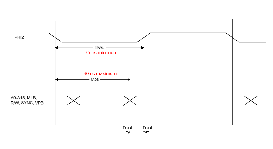
PHI2 and tADS.png [ 11.24 KiB | Viewed 836 times ]

Returning to the actual, original cause of my quibble, I believe Banedon was asking why we qualify RAM write-enable with Ø2. As I explained in my post Thursday, the answer is...
If you write-enable RAM or I/O while Ø2 is still low the target device will see an address bus that is in a state of flux -- not
BigDumbDinosaur wrote:
If you write-enable RAM or I/O while Ø2 is still low the target device will see a data bus that is in a state of flux.


However, the following is correct:
BigDumbDinosaur wrote:
If you remove the 65C816-specific outputs from the discussion you are looking at essentially the same timing model as that of the 65C02.
When running near maximum speed, '02 systems and '816 systems both take almost all of the Ø2-low time to produce a valid address; prior to that the address is garbage. And for write cycles they take almost all of the Ø2-high time to produce valid write data; prior to that the write data is garbage -- and that's normal; static RAM and 65xx peripherals can tolerate that, even though write-enable is asserted throughout the period of flux.

-- Jeff

_________________
In 1988 my 65C02 got six new registers and 44 new full-speed instructions!
https://laughtonelectronics.com/Arcana/ ... mmary.html


Top
 Profile  
Reply with quote  
 Post subject: Re: Star Ground
PostPosted: Sat Jan 02, 2016 9:07 am 
Offline
User avatar

Joined: Thu May 28, 2009 9:46 pm
Posts: 8382
Location: Midwestern USA
Dr Jefyll wrote:
When running near maximum speed, '02 systems and '816 systems both take almost all of the Ø2-low time to produce a valid address; prior to that the address is garbage. And for write cycles they take almost all of the Ø2-high time to produce valid write data; prior to that the write data is garbage -- and that's normal; static RAM and 65xx peripherals can tolerate that, even though write-enable is asserted throughout the period of flux.

...and for non-65xx peripherals we have flops to generate wait-states. :D

_________________
x86?  We ain't got no x86.  We don't NEED no stinking x86!


Top
 Profile  
Reply with quote  
Display posts from previous:  Sort by  
Post new topic Reply to topic  [ 135 posts ]  Go to page Previous  1 ... 5, 6, 7, 8, 9

All times are UTC


Who is online

Users browsing this forum: No registered users and 35 guests


You cannot post new topics in this forum
You cannot reply to topics in this forum
You cannot edit your posts in this forum
You cannot delete your posts in this forum
You cannot post attachments in this forum

Search for:
Jump to: