Hi Guys!
Thanks for welcoming me to your community, back over in my question thread. The responses have been truly amazing and I am quickly feeling that this is a great little community!
You'll find that my project is pretty bare bones at the moment as I am a complete newbie to the W65C02 CPU. But growing up as a kid with the Commodore 64 in the 80's has made me very fond of the 6502/10.
My lofty goals are to make a full computer with VGA output. Before you say "Oh god, here we go

" don't stress, I'm in no rush and am in it for the long haul. And besides, I have already built the functional VGA board.

I started this project in what people would consider to be reverse order.
Attachment:
 a3.jpg [ 137.31 KiB | Viewed 1663 times ]
Now we have that out of the way. I have started the CPU side of things by being very minimalistic, mainly because I am new to this side of things and will be very much experimenting with timings etc, until I get a firm understanding of what keeps the W65C02 happy. If it's happy, I'm happy!

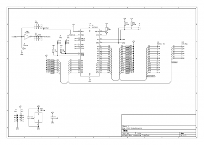
This is the bare bones circuit that I have started with, that I will expand upon.
Attachment:
 a1.png [ 80.82 KiB | Viewed 1663 times ]
The reason for the inverter there, is related to the 'BE' usage question, where I wanted to be able to invert the clock and put the CPU in to high-Z on the lower cycle. As I have found, it's not as simple as just doing that (did have some success though yesterday) so the inverter can be ignored.
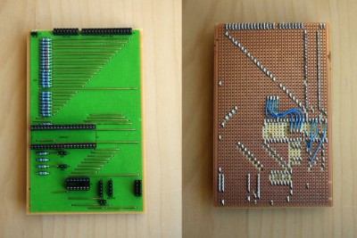
I created a stripboard, with heaps of header pins so I can connect other boards (like RAM etc.). I am pretty OCD with my stripboards. I tend to put the effort into going straight to stripboards as I am yet to find a breadboard that works reliably, they always seem to be a constant fight to get decent connections.
Attachment:
 a0.jpg [ 71.3 KiB | Viewed 1663 times ]
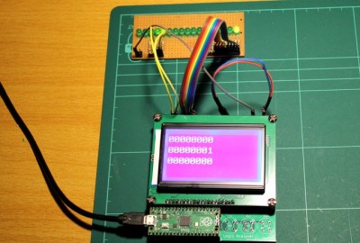
I have also made my own logic analyser, which I am monitoring the data and address bus with, and also acts as the clock to the 6502. Here's a pic of when I put it together after receiving the boards back from PCBWay after designing them. In the pic, I was just testing all of the I/O's to make sure it worked as planned, which it did!

Attachment:
 a4.jpg [ 65.87 KiB | Viewed 1663 times ]
The CPU gets it's ROM/RAM from another board I made which I call "FlashRAM 128". I needed a nice and easy way to be able to get programs to run on the 6502. It has a Raspberry Pi Pico, which pre-populates the RAM with whatever I want on it. It also holds the CPU in high-z, then resets it.
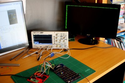
Here it is pre-loading the RAM on the aforementioned VGA card during early testing. The FlashRAM is the red board the VGA is two blue boards hooked together.
Attachment:
 a5.jpg [ 119.17 KiB | Viewed 1663 times ]
The 'FlashRAM' can either house a 128KB ram chip or can talk to external directly RAM.
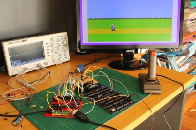
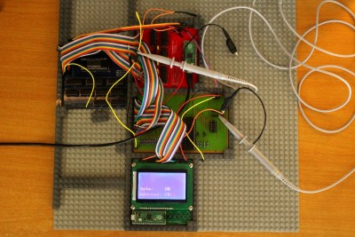
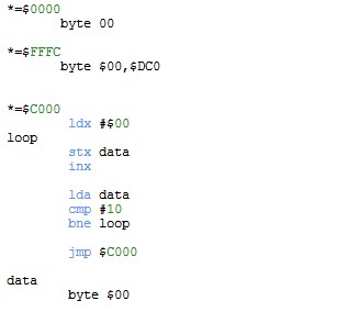
So here it is in its present form, all interconnected. I am dumping the program directly on to the VGA RAM board (holding the rest of the VGA boards circuit in high-z, so the CPU has exclusive use right now) and it is all happy running a simple program at around 2 Hz.
Attachment:
 a6.jpg [ 252.59 KiB | Viewed 1663 times ]
Attachment:
 a7.jpg [ 10.43 KiB | Viewed 1663 times ]
I know I'm not going to win any speed records with the current setup, it's purely to gain confidence and understanding of how the 6502 ticks.
So there you go! A fairly long winded first post. But hopefully this will give a bit of an insight as to where I'm coming from. Not afraid to get my hands dirty and not afraid to put my hand up when I don't know something. Hehe!
All feedback and questions are welcome.

(Typo in the reset vector - should read $C0 not $DC0. I mustn't have hit save last night when I corrected that)


