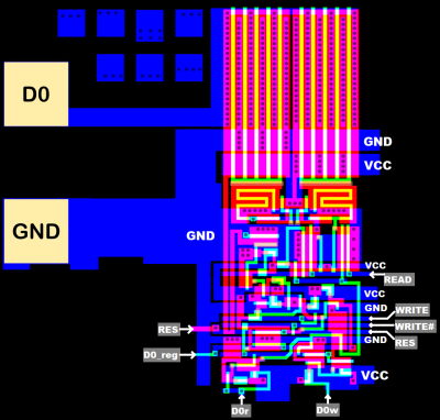
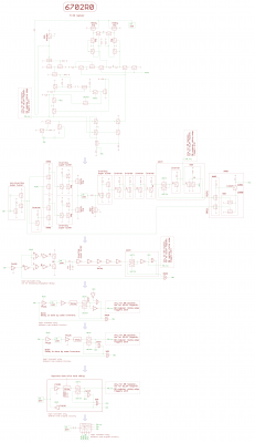
4) D0 register (plus D0 pad buffer\driver) located North West on the chip.
The shift register output goes through a non_inverting super buffer, then to the D0 pad driver,
and to a XNOR gate which feeds shift register output XNOR the low_active D0 data register output
back to the shift register input.
The D0 pad driver is nothing fancy, and its output is enabled with the high_active control signal READ.
The signal from the D0 pad goes through an inverting super buffer and through three inverters before entering the latch,
means that the data register latch stores D0 in inverted form.
//The delay which is built up by these inverters improves data write hold timing.
The edge detection circuitry which makes the shift registers shift by one Bit taps the high_active D0_reg signal from the D0 data register.
Note:
RES sets the low_active data register outputs to 0,
means the data register Bits are set during a RESET.
D0..D7 register (plus pad buffers\drivers) have identical layout on the chip, except for that D0_reg signal tapped from the D0 register.
Attachment:
 si6702_4_d0_register.png [ 93.72 KiB | Viewed 1975 times ]
Attachment:
 6702_4_d0_register.png [ 226.7 KiB | Viewed 1975 times ]
If you wonder why I'm drawing circles at the two FET inputs of the non_inverting super buffer which reads the shift register:
in the chip layout, we have vias there.
For D0..D7, there always is a metal trace between the two vias,
but to me it feels like the chip designers wanted to be able to change the functionality of that buffer by changing connections of that metal trace.


