6502.org Forum  Projects  Code  Documents  Tools  Forum
It is currently Wed May 08, 2024 5:07 pm

All times are UTC


Post new topic Reply to topic  [ 180 posts ]  Go to page Previous  1, 2, 3, 4, 5 ... 12  Next
Author Message
PostPosted: Sat Oct 22, 2022 1:12 pm 
Offline
User avatar

Joined: Tue Mar 05, 2013 4:31 am
Posts: 1373
Yes, that looks correct. If you look at my github page, your schematic is very similar to my old 65C02-SBC1, which uses the same 3 glue logic chips (with I/O at $FE00) and a 65C22 and 65C51 on a 2-board setup. Notes that schematic and PCB layout are done with ExpressPCB. Let us know how you make out.

_________________
Regards, KM
https://github.com/floobydust


Top
 Profile  
Reply with quote  
PostPosted: Sat Oct 22, 2022 4:40 pm 
Offline

Joined: Sat Apr 30, 2022 7:13 pm
Posts: 159
Location: Devon. UK
floobydust wrote:
Yes, that looks correct.
Excellent. Thank you. I will break out the wirewrapping tool tomorrow and let you know how I get on.


Top
 Profile  
Reply with quote  
PostPosted: Sun Oct 23, 2022 1:20 pm 
Offline

Joined: Sat Apr 30, 2022 7:13 pm
Posts: 159
Location: Devon. UK
Okay. I have eliminated U12 (part used 74HC00) using floobydust's logic. Thank you!

Still got the same odd problem with memory so I am now going to write a memory test program and see what it produces.


Top
 Profile  
Reply with quote  
PostPosted: Sun Oct 23, 2022 2:16 pm 
Offline
User avatar

Joined: Fri Dec 11, 2009 3:50 pm
Posts: 3354
Location: Ontario, Canada
adrianhudson wrote:
now going to write a memory test program and see what it produces.
Just a reminder that the parallel ports on your VIAs may come in handy as I/O. For example, your test program could scan memory addresses and then, upon encountering a fault, it could output the address in question (and perhaps also the defective data) to the VIA ports so you can be aware of the result.

Speaking of I/O, how were you made aware of the results when using NoICE? Does this tool talk to one of your serial ports? Is there a link or other doc you can share regarding NoICE?

But -- even though I'm the one who suggested the idea -- I have a feeling it's premature to delve deeper into test programs, which require considerable effort and yet have potential to become a rabbit hole. Firstly I'd wanna exhaust the possibilities of a wiring or other construction error (which seems rather plausible, given that we're dealing with a new build). :!:

When you tested the connections for continuity, were you testing from pin to pin on the IC sockets, or did you measure pin to pin on the actual chips themselves? The latter approach is preferable, as it's possible for an IC pin to fail to engage with corresponding insert of the socket. That can happen due to tarnish on either part, or it can happen that the IC pin has gotten folded underneath the IC rather than projecting into the socket insert as it should.

Finally, can you provide some photos of the board? No need to be shy; this is a learning process, after all. And some extra pairs of eyes could prove helpful.

-- Jeff

_________________
In 1988 my 65C02 got six new registers and 44 new full-speed instructions!
https://laughtonelectronics.com/Arcana/ ... mmary.html


Top
 Profile  
Reply with quote  
PostPosted: Sun Oct 23, 2022 4:06 pm 
Offline
User avatar

Joined: Tue Mar 05, 2013 4:31 am
Posts: 1373
Can you post some pics of the board showing both sides? Perhaps that might yield some new ideas on how to resolve the problem. Back in the day when I did wire-wrapping, I would run all power/ground lines first and install bypass caps on every chip. I also used much heavier non-wire-wrap wire for power and ground and these were all soldered to the socket pins.

The wire-wrapping was done only for the remaining interconnections, i.e., I never ran power or ground with wrire-wrap wire gauges.

_________________
Regards, KM
https://github.com/floobydust


Top
 Profile  
Reply with quote  
PostPosted: Sun Oct 23, 2022 4:33 pm 
Offline
User avatar

Joined: Fri Aug 30, 2002 1:09 am
Posts: 8432
Location: Southern California
floobydust wrote:
I also used much heavier non-wire-wrap wire for power and ground and these were all soldered to the socket pins.

The wire-wrapping was done only for the remaining interconnections, i.e., I never ran power or ground with wrire-wrap wire gauges.

There's a wire-inductance calculator at https://www.eeweb.com/tools/wire-self-i ... alculator/ .  Note that increasing the wire size has very little effect on inductance which is the real enemy.  For example, for a 6cm-long wire (about 2.5"), I started with .25mm diameter (the approximate diameter of WW wire), and got 73.4nH.  Then I multiplied the diameter by ten (and the cross-sectional area by 100), and got 46nH.  Multiplying the wire diameter by ten only reduced the inductance about 38%.  More realistically, going to a 22 AWG wire, or .64mm diameter, we get 62.2nH, giving a reduction in inductance of hardly over 15%.

Putting the power and ground wires down first puts them low on the WW pins, which is good because it shortens those connections; but beyond that, I would shift the focus not to larger-diameter wire, but rather to making the wire just barely long enough to reach its destination without being strained.  Buying pre-cut/pre-stripped WW wire and doing the swoopy curved wire paths is bad for performance, because of inductance.  Make sure the ground pins of all the ICs have the shortest practical connections, rather than one long daisychain that meanders around the board.

I kind of doubt that ground-connection inductance would cause the problem described above; but just carrying out good practice in these things will nevertheless avoid a lot of mysterious problems.

_________________
http://WilsonMinesCo.com/ lots of 6502 resources
The "second front page" is http://wilsonminesco.com/links.html .
What's an additional VIA among friends, anyhow?


Top
 Profile  
Reply with quote  
PostPosted: Sun Oct 23, 2022 9:34 pm 
Offline
User avatar

Joined: Wed Mar 01, 2017 8:54 pm
Posts: 660
Location: North-Germany
Perhaps you should try using Phi2(out) (p39) for timing and driving the I/O parts. All "classic" schematics use Phi2(out) as there is an unspecified delay between Phi0 and Phi2. Perhaps your /WE ends a little bit too soon causing the trouble.

good luck!


Top
 Profile  
Reply with quote  
PostPosted: Mon Oct 24, 2022 9:54 am 
Offline
User avatar

Joined: Sun Nov 07, 2021 4:11 pm
Posts: 101
Location: Toronto, Canada
Hello!

If you're using a modern 65C02 chip, you could take advantage of its fully static core and single-step through your program cycle by cycle; since you can hold each phase of the clock indefinitely, this would give you plenty of time to confirm that the circuit takes on the state you expect every time you perform a write to one of the problematic addresses.

IMO, you should consider trying to eliminate as many variables as possible; right now, the problem could be conceptual (timing), mechanical (a bad connection), or electrical (interference, etc.)… it's hard to pinpoint it when so many things could be going wrong. Perhaps removing every chip you don't need, loading a simple program that just attempts to write to the offending locations, and then single-stepping your way through it might reveal some important clues about what's going wrong, since you can check that the right chips are being selected, the address and data lines are set up correctly, and so on.

HTH!


—CC


Top
 Profile  
Reply with quote  
PostPosted: Sun Oct 30, 2022 2:45 pm 
Offline

Joined: Sat Apr 30, 2022 7:13 pm
Posts: 159
Location: Devon. UK
Wow everybody. I have been so engrossed trying to work out what the BEEP is going on that I didn't come back here to see if anyone else had replied - and you have. I am much obliged.

Some reples to your questions and suggestions:

I have been using the serial output to show errors. I'll come back to what I have found below.
NoICE is a Windows program that interfaces with a, I'll call it a monitor program on the 65C02 (and many other chips). The results are displayed on the screen and you can (amongst MANY other things) type into memory and get a response back keystroke by keystroke.

NoICE link: https://www.noicedebugger.com/ and https://www.noicedebugger.com/targets.html
Link direct to the 6502 NoICE page: https://www.noicedebugger.com/help/targets.htm#65C02

I have spent a considerable length of time checking every connection - not just simple continuity, but checking the resistance is negligable - from pin to pin on the chips - also checking every connection ONLY goes to where it is meant to go as well. Thats a lot of checks! I thought I had it when I found a tiny curl of wirewrap wire loose under a load of connections ... but no.

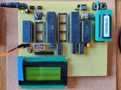
Photos are attached.

Other things I have done (from memory)
1. Replaced the memory chip... then...
2. Replaced all other chips. 65C02 down to 74 series.
3. checked power supply voltage and ripple etc. V a little high - 5.15V. Ripple very good - well, I think so.

I did write the memory test program and it indeed threw up more questions than it answered. Firstly, I think the recurring pattern of bad addresses were down to NoICE itself encountering memory problems in its own date area. Sometimes it will crash, sometimes other effects. I have stopped trying to use it as it is likely to cause confusion.

The memory test program simply fills memory (page 0 and page $02-$7E) with the same value, then it reads it all back and reports (over serial) which addresses don't match. Then it increments the value by 1 and repeats. So it fills memory and checks it with all 0 and then all 1 and so on (wraps back to 0) and repeats infinitely.

What this shows is that every few minutes an address is not written (or not read) correctly. Roughly 5 to 20 errors an hour.

In my ignorance, this implies some sort of timing error or interferance error. I can't see why it should be a timing error. I am only running at 1 MHz and the maximum propagation delay in the glue logic is only of the order of 50ns or so - I think.

As for interferance/crosstalk etc well, I can detect ripples in most address and data lines at clock frequency. They are there but not bad (that is a dangerous statement I guess - my 'scope is, lets say, "not the best". So, I should perhaps change that statement to "they are there and I don't THINK they are too bad").

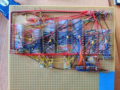
Okay, so now to construction. This machine is built on a piece of, I think its called perfboard(?). It has a pad round each hole on one side (that I have simply ignored). It therefore has no ground plane. Because of this I decided to connect each power and ground pin to TWO power distribution places one in the north east and one in the south west of the board and also connect every power and ground to its neigbor chip - so that gives a total of three connections for power and ground to each chip. I took Garth's suggestion of making like a spider's web to heart.

Garth, this is actually my second iteration of this board. The first had "swoopy" connections and was so ugly - and wouldn't run anyway - that I started again and did everything "shortest path" and straight.

CountChocula
Hello! I do have a test harness socket that allows me to monitor what's going on at a deep level - uses a good old Arduino to monitor a single stepped machine - but since the problem (or at least the manifestation of it with the memory test program) seems to have changed somewhat - I don't think it would really be possible to step through trillions of instructions. I did think of doing it but I don't think it would be practical.

"Removing every chip I don't need". From photos, you will see I have done this. In fact I had all but a single 6551 support chip out at one stage. No luck I am afraid.

So, where does that leave me? Well, I have ordered - from the USA - a new Twin Industries 8100 series (single ground plane) board as recommended by Garth and when it arrives I will- very probably - start again. In the meantime I will keep troubleshooting but with a) my equipment and b) my lack of knowledge/experience I suspect I am close to the limit of what I can do to find the problem.

GaBuZoMeu, you said about using Phi2(out) (p39) for timing and driving the I/O parts. I will have to get my head round that one. I havn't seen it done in any designs I have come across.

Some notes on the pictures. The odd thing near top left with a resistor soldered across it is an r2c attached real time clock. Connected to one of the VIAs. its not shown on the schematic. The display is not shown either also connected to VIA1

The sets of posts extreme top right and bottom left (back view) are for power distribution. As mentioned above all (well, most) chips' +V and GND are connected to both of these. The distribution posts are connected via the black and red wires along the top and down the left hand side (on the back view).
Oh and I have only connected to pin headers on 1 each of the 6551 and 6522 chips - If I ever get it working I will complete the I/O connections
Attachment:
IMG_20221030_133604.jpg
IMG_20221030_133604.jpg [ 1.8 MiB | Viewed 775 times ]

Attachment:
IMG_20221030_133634.jpg
IMG_20221030_133634.jpg [ 2.51 MiB | Viewed 775 times ]


Top
 Profile  
Reply with quote  
PostPosted: Mon Oct 31, 2022 1:21 am 
Offline

Joined: Wed Jun 23, 2021 8:02 am
Posts: 165
When you say you get roughly 5 - 20 errors per hour, do the errors always occur at the same RAM addresses or is the address completely random? Do they occur with particular data values? Is there any pattern to the corruption which occurs (e.g. always the same bit flipped?). Is it the write or the read which fails? You can tell by modifying your test program so if an error is noticed you repeat the read and see if you get the same value again or if the second read gives the correct value.

Regarding the board photos, the leads on the bypass capacitors seem quite long, but it's not obvious how you could make them much shorter without completely rebuilding everything and somehow getting a ground plane in there.


Top
 Profile  
Reply with quote  
PostPosted: Mon Oct 31, 2022 5:30 am 
Offline
User avatar

Joined: Fri Dec 11, 2009 3:50 pm
Posts: 3354
Location: Ontario, Canada
adrianhudson wrote:
Because of this I decided to connect each power and ground pin to TWO power distribution places one in the north east and one in the south west of the board and also connect every power and ground to its neigbor chip - so that gives a total of three connections for power and ground to each chip. I took Garth's suggestion of making like a spider's web to heart.

The part that jumps out at me here is, "and also connect every power and ground to its neighbor chip." I'm glad to hear about the "neighbor" connections, but I suspect you may not have taken the idea far enough. In regard to power and ground, it's the connections to neighboring chips that are crucial (and not so much the connections to the power distribution places). More on that in the first few paragraphs of this post (which Garth cites in the fourth paragraph of his article).

Try to establish a grid, which ensures that each chip has connections to its neighbors to the East, West, North and South. Of course, chips on the perimeter or in the corner have only three or two neighbors, not four. But as much as possible you wanna connect to all points of the compass. Each ground pin should ideally connect to the ground pin of the chips to the N, S, E and W.... and likewise each power pin should ideally connect to the ground pin of the chips to the N, S, E and W.

From the photo I can't tell how near or far this is from being true. But it wouldn't take much work to add any wires that are missing, and it's possible (though hardly guaranteed) that this might correct your problem.

Worth a try, I'd say! It's surely a lot easier than building a new board. (And you've already done a very nice job, BTW! -- congrats on your project!)

-- Jeff

_________________
In 1988 my 65C02 got six new registers and 44 new full-speed instructions!
https://laughtonelectronics.com/Arcana/ ... mmary.html


Top
 Profile  
Reply with quote  
PostPosted: Mon Oct 31, 2022 7:08 pm 
Offline

Joined: Sat Apr 30, 2022 7:13 pm
Posts: 159
Location: Devon. UK
kernelthread wrote:
When you say you get roughly 5 - 20 errors per hour, do the errors always occur at the same RAM addresses or is the address completely random? Do they occur with particular data values? Is there any pattern to the corruption which occurs (e.g. always the same bit flipped?). Is it the write or the read which fails? You can tell by modifying your test program so if an error is noticed you repeat the read and see if you get the same value again or if the second read gives the correct value.

Regarding the board photos, the leads on the bypass capacitors seem quite long, but it's not obvious how you could make them much shorter without completely rebuilding everything and somehow getting a ground plane in there.

It seems to be random. It also seems that it is the write that didn't work since, when I find a mismatch, I output the address, what I expect to find at that address and what I actually find at the address. Since I am storing an increasing set of values to all memory e.g. all $00, and check, all $01 and check all $02 and check, I "usually" (I haven't double checked it is "always", but it might be) get the preceeding value, I get, say, $54 when I should get a $55. By the way, the program occaisionally crashes, I guess through the stack itself becoming corrupted.

On the cap leads, yes, but they are as short as I can make them.


Last edited by adrianhudson on Mon Oct 31, 2022 7:21 pm, edited 1 time in total.

Top
 Profile  
Reply with quote  
PostPosted: Mon Oct 31, 2022 7:18 pm 
Offline

Joined: Sat Apr 30, 2022 7:13 pm
Posts: 159
Location: Devon. UK
Dr Jefyll wrote:
... Try to establish a grid, which ensures that each chip has connections to its neighbors to the East, West, North and South. Of course, chips on the perimeter or in the corner have only three or two neighbors, not four. But as much as possible you wanna connect to all points of the compass. Each ground pin should ideally connect to the ground pin of the chips to the N, S, E and W.... and likewise each power pin should ideally connect to the ground pin of the chips to the N, S, E and W.
...
Worth a try, I'd say! It's surely a lot easier than building a new board. (And you've already done a very nice job, BTW! -- congrats on your project!)
-- Jeff

Will do! Will report back. And thanks for continuing to take time to help. And also thanks for your comments on the physical board. Its the first wire wrap I have done and the first of this sort of project - IC layout etc. I have no proper idea of what I am doing, I have just tried to follow advice and tidbits I have found. There is NO substitute, really, for learning from someone else - either informally or formally. Learning from the Internet aught to be easy, but is actually quite hard.

One question. I have seen the use of tiny ferrite beads on sertain conductors buy some people. Might this be a good idea on chip +5V lines - say to the oscillator cans - to attempt to reduce, I''l call it "interference"?


Top
 Profile  
Reply with quote  
PostPosted: Mon Oct 31, 2022 9:11 pm 
Offline

Joined: Sat Apr 30, 2022 7:13 pm
Posts: 159
Location: Devon. UK
Well, here's a thing.

I realised on looking at the spider's web power and gnd interconnects that I had missed off direct interconnects between the 65C02 and RAM and ROM chips. There wasn't enough heighton the wrap pins to do 65C02 to RAM AND 65C02 to ROM to I added:

+5V 65C02--->RAM--->ROM
GND 65C02--->RAM--->ROM

i.e. 4 extra wires.

And damn me, it makes it WORSE. The memory test program starts, issues a CR and LF to the 6551 and then it is supposed to go on to print a banner before starting its work. It does the CRLF and then never gets any further before crashing.

I took the extra wires off and its back working again. How can that BE???

I am beginning to be seriously demoralised with this thing. :-(


Top
 Profile  
Reply with quote  
PostPosted: Mon Oct 31, 2022 9:14 pm 
Offline
User avatar

Joined: Thu Dec 11, 2008 1:28 pm
Posts: 10800
Location: England
It's possible this will help - finding a problem which happens in seconds is a lot easier than finding one which happens in hours.


Top
 Profile  
Reply with quote  
Display posts from previous:  Sort by  
Post new topic Reply to topic  [ 180 posts ]  Go to page Previous  1, 2, 3, 4, 5 ... 12  Next

All times are UTC


Who is online

Users browsing this forum: No registered users and 5 guests


You cannot post new topics in this forum
You cannot reply to topics in this forum
You cannot edit your posts in this forum
You cannot delete your posts in this forum
You cannot post attachments in this forum

Search for:
Jump to: