Simple Question: 65c816 - Part Deux!
Posted: Fri Sep 17, 2021 4:27 pm
This is the second entry pertinent to this thread: viewtopic.php?f=1&t=6777
So I had some time, and I implemented a design using this, from BigDumbDinosaur, for decoding read and write: viewtopic.php?f=1&t=6777#p87016
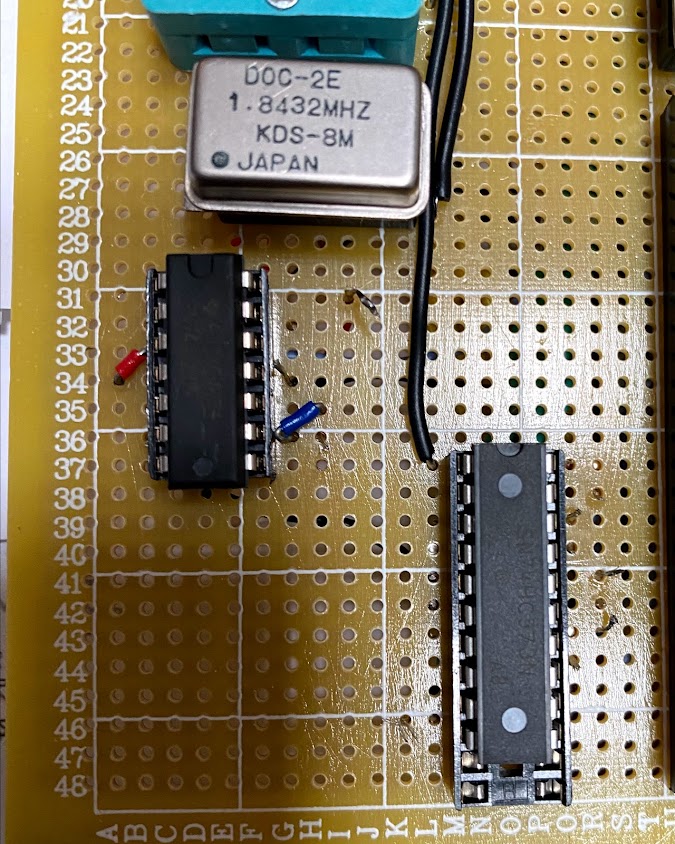
I implemented this in one 74AC00.
https://photos.google.com/u/2/share/AF1 ... RMZmxFOERn
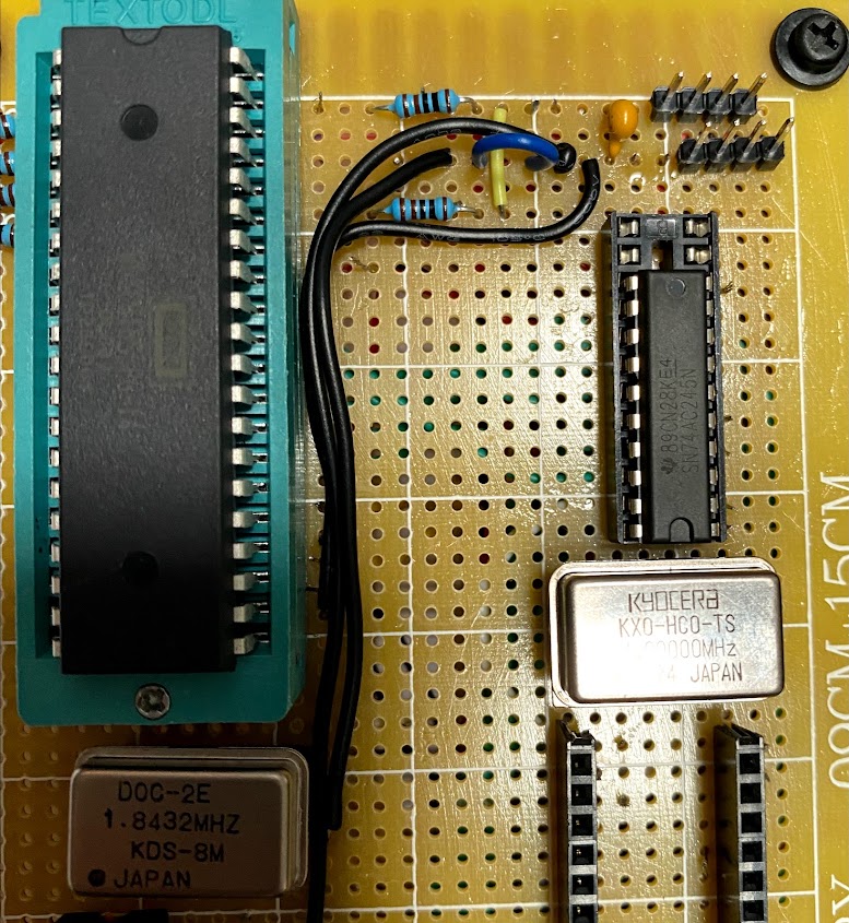
I used Dr. Jefyll's connection scheme: viewtopic.php?f=1&t=6777#p87025
It goes through a 74AC245: https://photos.google.com/u/2/share/AF1 ... RMZmxFOERn
As you guys said, the B side faces the CPU and the A side faces outward to the bus.
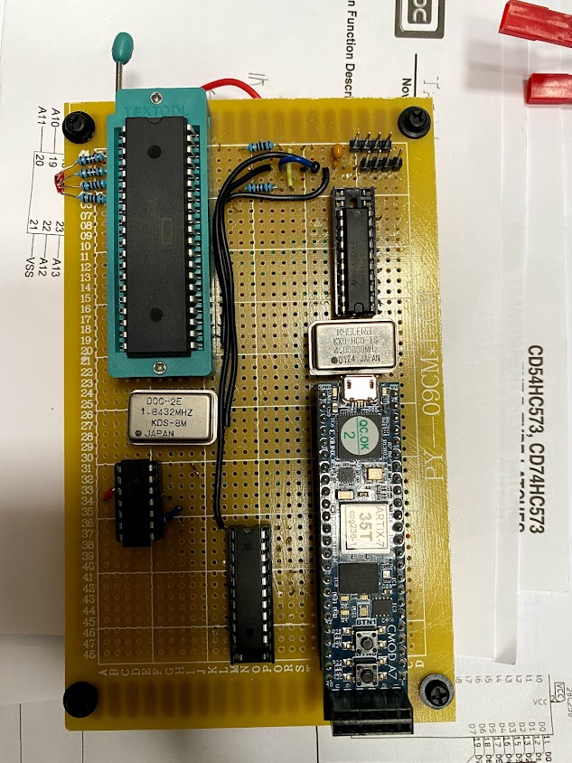
Then, I implemented the bank address capture scheme found in the 65c816 data sheet, through a 74HC573: https://photos.google.com/u/2/share/AF1 ... RMZmxFOERn
Then I ran all the lines (data out from the '245, bank addresses from the '573, addresses from the cpu, and /rd and /wr from the '00) into a CMOD A7 35T (has 512k SRAM): https://photos.google.com/u/2/share/AF1 ... RMZmxFOERn
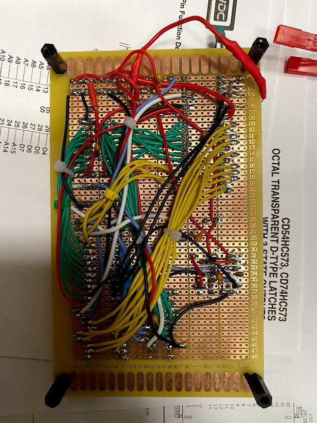
I was extremely careful with the wiring, testing and retesting with the multimeter as a soldered. I also ran a 4mhz clock into the FPGA for phi2 and a 1.8432mhz into the FPGA for LIV2's soft ACIA.
I tested extensively with my multimeter and logic probe, and I caught one issue, but everything checks out now.
My usual verilog tricks don't seem to work. Even with all those signals generated in hardware, I cannot get it to play nice. Can someone propose a verilog scheme that might work? I'm just trying to hook the cpu signals into the internal SRAM and LIV2's acia for basic testing and verification.
I have the data signals from Port A of the '245.
I have the bank signals from the '573.
I have all the processor signals.
And I have the /rd and /wr from the '00.
Jonathan
PS The specs for the CMOD A7 35T can be found here: https://digilent.com/reference/programm ... d-a7/start
So I had some time, and I implemented a design using this, from BigDumbDinosaur, for decoding read and write: viewtopic.php?f=1&t=6777#p87016
I implemented this in one 74AC00.
https://photos.google.com/u/2/share/AF1 ... RMZmxFOERn
I used Dr. Jefyll's connection scheme: viewtopic.php?f=1&t=6777#p87025
It goes through a 74AC245: https://photos.google.com/u/2/share/AF1 ... RMZmxFOERn
As you guys said, the B side faces the CPU and the A side faces outward to the bus.
Then, I implemented the bank address capture scheme found in the 65c816 data sheet, through a 74HC573: https://photos.google.com/u/2/share/AF1 ... RMZmxFOERn
Then I ran all the lines (data out from the '245, bank addresses from the '573, addresses from the cpu, and /rd and /wr from the '00) into a CMOD A7 35T (has 512k SRAM): https://photos.google.com/u/2/share/AF1 ... RMZmxFOERn
I was extremely careful with the wiring, testing and retesting with the multimeter as a soldered. I also ran a 4mhz clock into the FPGA for phi2 and a 1.8432mhz into the FPGA for LIV2's soft ACIA.
I tested extensively with my multimeter and logic probe, and I caught one issue, but everything checks out now.
My usual verilog tricks don't seem to work. Even with all those signals generated in hardware, I cannot get it to play nice. Can someone propose a verilog scheme that might work? I'm just trying to hook the cpu signals into the internal SRAM and LIV2's acia for basic testing and verification.
I have the data signals from Port A of the '245.
I have the bank signals from the '573.
I have all the processor signals.
And I have the /rd and /wr from the '00.
Jonathan
PS The specs for the CMOD A7 35T can be found here: https://digilent.com/reference/programm ... d-a7/start