Page 1 of 2
VIA 6522 SHIFT External Clock reverse engineered schematics
Posted: Sat Apr 24, 2021 12:48 am
by ijor
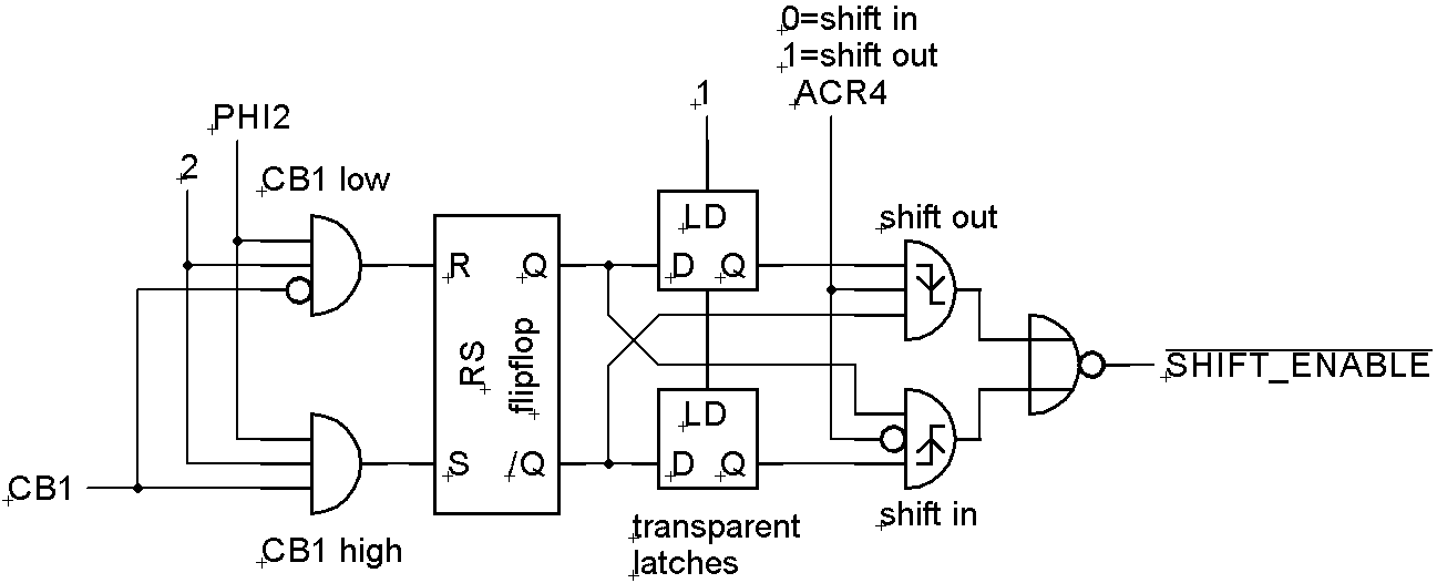
I don't know much about the 6522. No of the systems that I specialize uses a VIA. But I recently found out about the SHIFT external clock bug, that happens to be almost exactly the same as a chip that I do am familiar. So I was very curious and reverse engineered the VIA 6522 external clock logic.
Below is a link to the SHIFT external clock logic, reverse eginereed from die shots. You can see that synchronization is far from being foolproof:
https://github.com/ijor/VIA6522/blob/ma ... tector.png
One interesting point. The output of this edge detector enables the shifting. There is no clock mux that selects between the external and the internal clocks depending on the settings of the ACR registers. That was initially a surprise, and it might be non obvious how it could work like that at all. But after some though you realize that a clock mux is not really needed and the expected, documented behaviour works perfectly fine like this.
Re: VIA 6522 SHIFT External Clock reverse engineered schemat
Posted: Sat Apr 24, 2021 1:17 am
by GARTHWILSON
Fortunately it's only in the one SR mode (out of seven) and won't affect most users. It seems a cryin' shame that after 40+ years it still has not been fixed though. There's a work-around in the "Tip of the Day" column, #8, at viewtopic.php?p=2310#p2310 .
Re: VIA 6522 SHIFT External Clock reverse engineered schemat
Posted: Sat Apr 24, 2021 2:18 am
by ijor
Fortunately it's only in the one SR mode (out of seven) and won't affect most users.
Why one mode only? It should affect both modes that use an external clock, shift in (mode 011) and shift out (mode 111).
Anyway, it wasn't my intention at all to complain or to criticize the VIA

I just thought it would be interesting to show the exact logic that produces the bug, and perhaps even more interesting to mention the lack of a clock mux that might have side effects under some conditions.
Re: VIA 6522 SHIFT External Clock reverse engineered schemat
Posted: Sat Apr 24, 2021 3:41 am
by GARTHWILSON
Why one mode only? It should affect both modes that use an external clock, shift in (mode 011) and shift out (mode 111).
Re: VIA 6522 SHIFT External Clock reverse engineered schemat
Posted: Sat Apr 24, 2021 4:22 am
by enso
Garth,
Could you clarify your head-slapping realization in the tutorial?
Do you mean to always let the recipient do the shifting with their own, safe clock?
Re: VIA 6522 SHIFT External Clock reverse engineered schemat
Posted: Sat Apr 24, 2021 5:23 am
by GARTHWILSON
Ok, I went back to Synertek's ap. note AN-5 which is where I got the explanation after I first had the problem of occasionally dropping bits, and found that sure enough, it does also mention mode 111. I had missed that earlier, since I was only looking for a solution for mode 011. I just now edited both the SS22 article and the Tip of the Day post. I've been using 011 with the FF for many years, in something that just works, so I never have to think about it.
So if the clock is external, the only way to do the shifting, in or out, is to use the FF.
Re: VIA 6522 SHIFT External Clock reverse engineered schemat
Posted: Sun Apr 25, 2021 7:03 am
by BigEd
... So I was very curious and reverse engineered the VIA 6522 external clock logic.
Below is a link to the SHIFT external clock logic, reverse eginereed from die shots. You can see that synchronization is far from being foolproof:
https://github.com/ijor/VIA6522/blob/ma ... tector.png
Excellent work Ijor! I'm sure many have wondered about the machinery inside, that's responsible for this peculiarity!
Re: VIA 6522 SHIFT External Clock reverse engineered schemat
Posted: Mon Apr 26, 2021 2:06 pm
by ttlworks
Ijor, nice work.
CB1 is sampled when the non_overlapping clock 2 is high (during PHI2=high),
to synchronize the external CB1 clock signal with PHI2.
This sure can cause problems if the external clock signal at CB1 is from a different clock domain
(not generated by something running with the same PHI2 clock than the 6522).
IMHO it would have been better to generate the shift register clock directly from CB1 to get around such problems,
but this would have created another problem: synchronizing the parallel shift register outputs with PHI2
(what would have taken more transistors and more chip space).
Felt a need to re_draw your schematics, and I'm adding a monochrome picture for those who happen to be color blind:
- 6522_sr_clk_monochrome.png (5.83 KiB) Viewed 1900 times
Re: VIA 6522 SHIFT External Clock reverse engineered schemat
Posted: Mon Apr 26, 2021 6:25 pm
by ijor
Felt a need to re_draw your schematics
Sure. I actually appreciate it because, as it might be obvious, I'm not very good at drawing schematics.
A small comment though. The gates you draw as transparent latches are actually dynamic delays, or dynamic latches if you want. They retain the state only by capacitance and they will discharge eventually if not refreshed. Of course, this chip has plenty of those dynamic cells and obviously it is not fully static. I realize you already knew that, but I think it should be somehow noted in the schematics.
Re: VIA 6522 SHIFT External Clock reverse engineered schemat
Posted: Tue Apr 27, 2021 5:34 am
by ttlworks
I'm aware of the dynamic latches, already had that game when
dissecting the 8701 clock generator chip.
I think that the schematic is more easy to understand when drawing transparent latches instead of dynamic latches.
Also, I think it simplifies things for those who might want to try simulating the circuitry.
Ijor, any plans to go for the rest of the 6522 silicon ?
Unfortunately, there don't seem to be polygonized pictures of the 6522 silicon in the internet.
Polygonized pictures would be very helpful for reverse engineering the chip.
Re: VIA 6522 SHIFT External Clock reverse engineered schemat
Posted: Thu Apr 29, 2021 12:26 am
by ijor
I think that the schematic is more easy to understand when drawing transparent latches instead of dynamic latches.
Also, I think it simplifies things for those who might want to try simulating the circuitry.
Well, might be a matter of personal preferences. But be aware that a dynamic cell can't always be modeled and replaced with a transparent latch. Sometimes the capacitive feature is important, such as when you have multiple of those transistors in parallel. In such a case, multiple transparent latches that constantly drive their outputs would create contention and would not work.
Ijor, any plans to go for the rest of the 6522 silicon ?
The layout of this chip is rather straightforward to analyze, so I might. But it would take some time as, unfortunately, it is not currently at the top of my priorities.
Re: VIA 6522 SHIFT External Clock reverse engineered schemat
Posted: Thu Apr 29, 2021 6:03 am
by ttlworks
It actually is a matter of personal preferences.
I think that I'm aware of the importance of the capacitive features.
Thanks for pointing that out, not all of the readers might be aware of it.
If you would be trying to analyze the chip,
I would be trying to help if my spare time permits this.
I already had helped with the dissection of the SID chip,
and some years ago I did an
experimental TTL implementation of the 6522.
Re: VIA 6522 SHIFT External Clock reverse engineered schemat
Posted: Thu Apr 29, 2021 1:43 pm
by ijor
I think that I'm aware of the importance of the capacitive features. Thanks for pointing that out, not all of the readers might be aware of it.
I understand. Sorry that I might have implied you are not familiar with this kind of logic.
Impressive work!
Re: VIA 6522 SHIFT External Clock reverse engineered schemat
Posted: Fri Apr 30, 2021 8:03 am
by ttlworks
Thanks for the kind words.
The schematics for the experimental TTL 6522 implementation are
here.
Of course, to me a
TTL implementation of the 6526 would be more interesting, because I'm supporting the
C74 project.
But because nobody aims at dissecting the 6526 chip yet, dissecting the 6522 chip would be a nice start to begin with.
VIA 6522 chip select bug
Posted: Tue May 04, 2021 5:51 pm
by ijor
Quote from wikipedia:
Aside from the aforementioned shift register bug, there was a potential register corruption problem that usually only occurred in systems using the 6522 with a microprocessor having a non-6502 bus architecture, such as a Motorola 68000. If the address lines changed while chip select was low (inactive) but the ϕ2 clock input was high (active), register contents could be changed despite the fact that the chip was not selected. This was fixed in some but not all of the CMOS versions.
Any further details about this,
supposed, bug?
According to what I see, there is no such bug. Of course, VIA assumes a 6502 bus protocol and expects the CPU interface signals to be synchronous to the system clock. Timing issues could happen if the bus signals violate the setup or hold specifications regarding the main clock. But this is about the same as almost every other 650X peripheral, including i.e., PIA. Those chips were not designed for a full asynchronous bus interface. They perform the writing synchronous to the system clock, not synchronous to the chip select signal(s) as other chips do.
The bug description seems to suggest that register corruption might happen even if the chip was not selected at all, just by the fact that the address lines change at the wrong time. This doesn't seem to be accurate. Register corruption might happen only
if the chip is selected but the address lines change before the clock edge (hence violating hold time specifications).