Page 1 of 2
Don't Do What I Just Did
Posted: Wed Mar 03, 2021 10:43 am
by sci4me
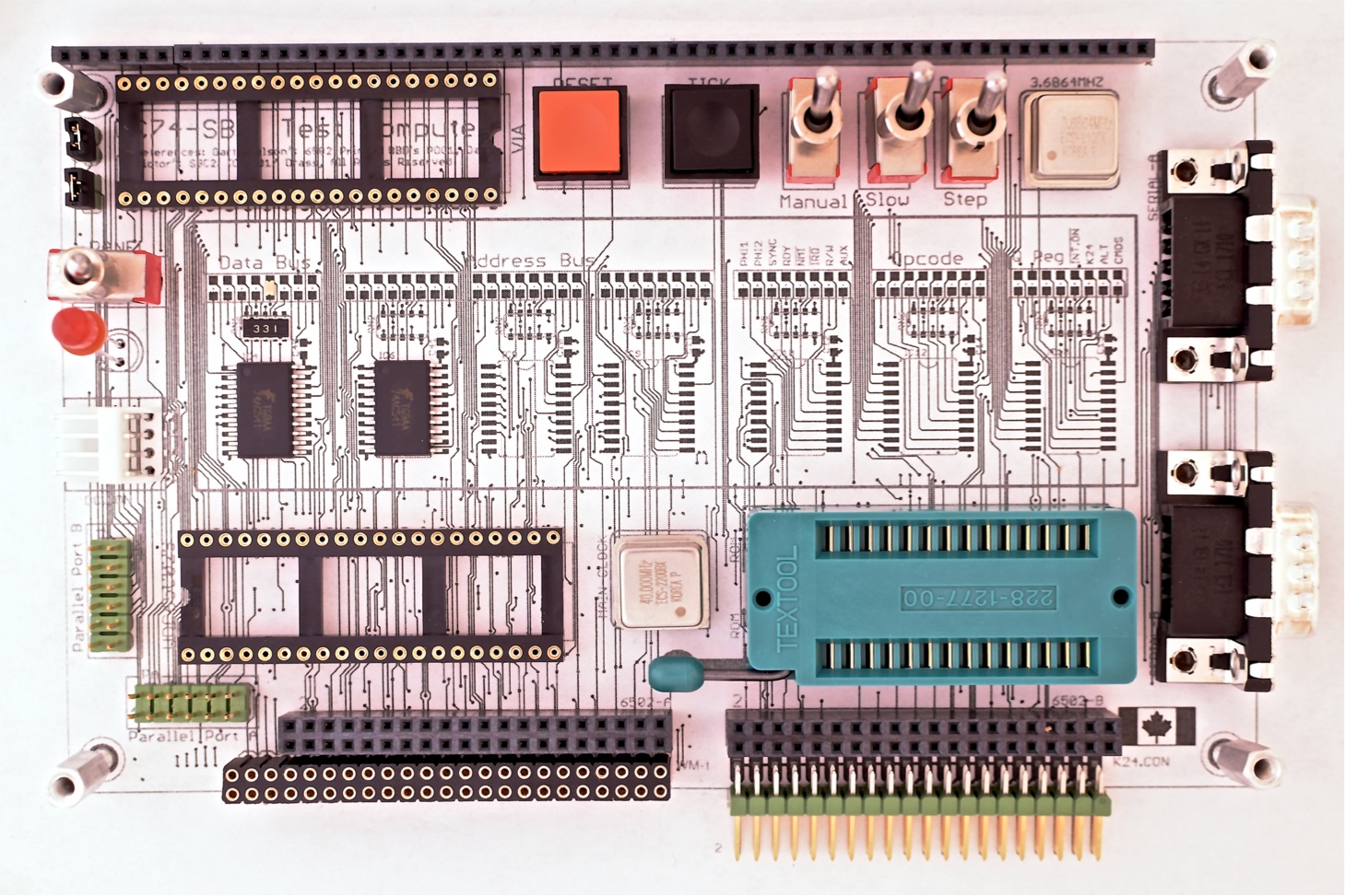
So I randomly decided that I wanted to try my hand at SMD/SMT electronics for the first time ever. I had a design for a simple 65(c)02 SBC, nothing particularly unique there, and I knew the WDC parts came in QFP and PLCC packages, so I just went ahead and converted the design to use the SMT parts, along with a few minor changes/additions. For my first SMT board layout I think it turned out alright, although I definitely learned a lot along the way. Finally today (yesterday now) the boards arrived and I was quite thrilled with how they turned out, other than a minor silkscreen mistake.
But then it all came crashing down. I tried so hard and got so far, but in the end it didn't even matter. I made a rather awful mistake: I used a completely incorrect footprint for the 65C02 and 65C22s! Doh!
Thankfully though, I ended up with some unique looking coasters along with confirmation that some of the additions I made, to do with the USB interface, seem to work. Not worth the ninety bucks or so, but hey, what can I say, I'm a computer programmer, not an engineer

Re: Don't Do What I Just Did
Posted: Wed Mar 03, 2021 12:09 pm
by BigEd
Oh no! That's a shame. It is one of the big differences between software and electronics: a revision or a mistake can be much more expensive in hardware. (One of the reasons that programmable logic is very handy, as reprogramming it is quick and not disruptive.)
Other than carefully checking before going ahead to manufacture - perhaps ideally get someone else to cast an eye over your work - just accepting that some of the time, maybe most of the time, your first design won't be your final design. And so that affects your idea of how much your project is going to cost.
(The cost of PCBs has come right down, but it's still a function of how big the board is, how many layers, and how rapid a turnaround you want.)
Re: Don't Do What I Just Did
Posted: Wed Mar 03, 2021 2:10 pm
by cbmeeks
I was quite thrilled with how they turned out, other than a minor silkscreen mistake.
Was the mistake the scantly-clad lady on the front? LOL
I actually like the layout of the board. Oh, I'm also not a hardware engineer but a software engineer. So yeah...happened to me too. My first SBC is a small green coaster now. But hey...at least it has my name on it for future generations to mock...er...study. lol
Re: Don't Do What I Just Did
Posted: Wed Mar 03, 2021 5:54 pm
by BigDumbDinosaur
Urk!
I haven't made that mistake...yet. However, I've made other that were as egregious. You could hang the bad PCBs on the wall and call them modern art. Or perhaps take them out back along with your gun and do some plinking. 
BTW, I recommend you lose the filled planes (aka ground pours). All those are doing for you is adding unwanted parasitic capacitance.
Re: Don't Do What I Just Did
Posted: Wed Mar 03, 2021 6:03 pm
by BigDumbDinosaur
My first SBC is a small green coaster now.
POC V1.0 came close to achieving coaster status but I was able to rescue it with three bodge wires and some X-Acto knife work. POC V1.2 had a component footprint that turned out to be wrong. I was able to recover from that using a combination of the trusty X-Acto knife and some funny wiring. However, there's no rescuing a layout with wrong component footprints with a lot of pins. 
Re: Don't Do What I Just Did
Posted: Wed Mar 03, 2021 6:04 pm
by Drass
I was saved from a similar fate by a comment I read somewhere about using a scale-accurate printout of the PCB to check all the footprints prior to sending the Gerbers off. It's also helpful in making sure the housings of connectors and other gadgets don't step on each other, which is unfortunately is something I learned only after being bitten by it. (In the pic below, the bottom left pin header is too close to the IC socket for a ribbon cable connector to fit comfortably. This printout came from Eagle CAD but I suspect most other tools would have a similar function).
Re: Don't Do What I Just Did
Posted: Wed Mar 03, 2021 6:21 pm
by BigDumbDinosaur
I was saved from a similar fate by a comment I read somewhere about using a scale-accurate printout of the PCB to check all the footprints prior to sending the Gerbers off.
That might have been me who advised that. When I did the layout for POC V1.0 (nearly 12 years ago—where did the time go?) I printed an exact-size rendition of the PCB and set components on it to check fit. Doing so resulted in some adjustments when it became clear assembly would be a problem. Unfortunately, it didn't save me from some layout errors and a design error. 
Re: Don't Do What I Just Did
Posted: Wed Mar 03, 2021 6:23 pm
by sci4me
Other than carefully checking before going ahead to manufacture
Yep, no doubt I'll be doing this a bit more thoroughly from now on.
Interestingly, I found that the WDC datasheets, as far as I can tell, do not specify a single thing about the physical device packages, such as dimensions; they only specify 'DIP', 'QFP', and 'PLCC' -- unless I'm just missing something. I actually had to find the dimensions on a
StackExchange post. Not to blame WDC in any way, but it is odd; I've never seen any other datasheets like that that I can think of.
Was the mistake the scantly-clad lady on the front?
The labeling on the left side GPIO connector is missing power and ground as it is on the right side.
I recommend you lose the filled planes (aka ground pours). All those are doing for you is adding unwanted parasitic capacitance.
This is something I've been wondering about but haven't done enough research on. I was under the impression that it wouldn't be any different, essentially, than the actual ground plane...
I have signals on top and bottom and just below top I have power and ground below that.
In all honesty the aesthetic is not an insignificant part of why I did add those ground fills on top and bottom, which seemed reasonable given my assumption that it would have little effect on the function of the board. Definitely an area I'd like more solid info about, just haven't dug into that yet.
I was able to recover from that using a combination of the trusty X-Acto knife and some funny wiring.
I briefly considered trying to find some hacky way to get the chips connected but really, I figure I'd be less frustrated by just re-spinning the board
I was saved from a similar fate by a comment I read somewhere about using a scale-accurate printout of the PCB to check all the footprints prior to sending the Gerbers off.
Will definitely keep this one in my back pocket! I even have a printer, never used the thing though lol.
As painful as a mistake this egregious is to make, at least it wasn't entirely a waste. I did confirm that the FTDI chip and USB/external power setup works, so I guess that counts for something. That and experience.
Rev. 2 will be the one

Re: Don't Do What I Just Did
Posted: Wed Mar 03, 2021 6:38 pm
by BigDumbDinosaur
Other than carefully checking before going ahead to manufacture
Yep, no doubt I'll be doing this a bit more thoroughly from now on.
As we often say in the metalworking hobby, measure twice and cut once. That's especially true if using titanium.
Interestingly, I found that the WDC datasheets, as far as I can tell, do not specify a single thing about the physical device packages, such as dimensions...
Sketchy documentation has long been a problem with WDC. The current data sheets aren't too bad, but you do need to be careful to read in between the lines.
I recommend you lose the filled planes (aka ground pours). All those are doing for you is adding unwanted parasitic capacitance.
This is something I've been wondering about but haven't done enough research on. I was under the impression that it wouldn't be any different, essentially, than the actual ground plane...
I have signals on top and bottom and just below top I have power and ground below that.
In all honesty the aesthetic is not an insignificant part of why I did add those ground fills on top and bottom, which seemed reasonable given my assumption that it would have little effect on the function of the board. Definitely an area I'd like more solid info about, just haven't dug into that yet.
We have an extensive topic on designing for high speed performance. Among other things, the value of four-layer construction and the negatives of having filled planes are discussed. My POC V1.2 unit (most recent in the series) is running at 20 MHz on a four-layer board. There are no filled planes other than in areas where I am trying to suppress stray radiation (the Ø2 oscillator runs at 40 MHz).
Re: Don't Do What I Just Did
Posted: Wed Mar 03, 2021 8:17 pm
by floobydust
I started doing PCB 1:1 scale prints years ago... but carry it one step further. I mount the printed PCB paper on a piece of styrofoam and then poke holes for all of the components and place them to ensure everything fits... albeit SMT bits of course.
However, I once made a PCB and used the wrong gender for a DB-9 connector! Paper sizing fits fine, but it took some head-scratching to figure our why the serial port didn't work at work at first!
Re: Don't Do What I Just Did
Posted: Wed Mar 03, 2021 8:30 pm
by plasmo
Doing hardware for 35 years so I have made plenty of layout mistakes. In fact, even after retirement I still made some spectacular mistakes. Here are a couple in the last 3 years to entertain you:
pic 1: 68000 DIP is 900 mil wide, NOT 600mil
pic 2: shrink DIP64 pitch is 70 mil, not 75mil
Re: Don't Do What I Just Did
Posted: Wed Mar 03, 2021 8:33 pm
by cbmeeks
However, there's no rescuing a layout with wrong component footprints with a lot of pins.
Unless you can do some serious dead-bugging!
Re: Don't Do What I Just Did
Posted: Wed Mar 03, 2021 9:52 pm
by Drass
I was saved from a similar fate by a comment I read somewhere about using a scale-accurate printout of the PCB to check all the footprints prior to sending the Gerbers off.
That might have been me who advised that.
That seems to me very likely BDD. I recall studying your POC units carefully, and more than once applying your recommendations. All very much appreciated!

Re: Don't Do What I Just Did
Posted: Wed Mar 03, 2021 9:55 pm
by Drass
I still made some spectacular mistakes. Here are a couple in the last 3 years to entertain you:
These are great Plasmo. Thanks for sharing!
Re: Don't Do What I Just Did
Posted: Thu Mar 04, 2021 7:11 am
by BigDumbDinosaur
Doing hardware for 35 years so I have made plenty of layout mistakes. In fact, even after retirement I still made some spectacular mistakes. Here are a couple in the last 3 years to entertain you:
pic 1: 68000 DIP is 900 mil wide, NOT 600mil
pic 2: shrink DIP64 pitch is 70 mil, not 75mil
If you use a big enough hammer the parts might fit.