Page 1 of 2
Theorizing about interfacing a NMOS VIC-II with a 65cxx CPU.
Posted: Wed Aug 05, 2020 2:59 pm
by tokafondo
In a C64, the VIC-II controls the CPU, giving it the clock and stopping it
through RDY and AEC pins.
In a C64, the VIC-II receives two clock ticks. A "COLOR CLOCK" for the video
color generation, and a "DOT CLOCK" for its internal workings, where it gets
divided for external CPU clocking. A 8701 chip gets those clock given to the
VIC-II.
What about this?
Put a clock in a board of double the rate a 8701 needs to be fed with
(double of 14.31818 or 17.734472 Mhz).
Make the clock send: one tick to the 8701, and the other one to a 65c02/816
chip, so both the chips would receive its intended tick one each following
the other, alternately.
The VIC-II would behave as always, and the 65c02/816 would too. Both of them
would be able to access the RAM never at the same time, because their clocks
would never overlap.
But maybe that wouldn't stop the VIC-II to need being able to stop the CPU
to gets its reads during badlines, sprites and so.
Also, the VIC-II wouldn't be able to stand access for read or write to its
registers at such a high speed from the CPU (although the datasheet does not
list a "minimal" time for that - or I can't read a dataheet).
What do you think?
Re: Theorizing about interfacing a NMOS VIC-II with a 65cxx
Posted: Fri Aug 07, 2020 3:11 am
by brain
If I understand you correctly, you'd do this:
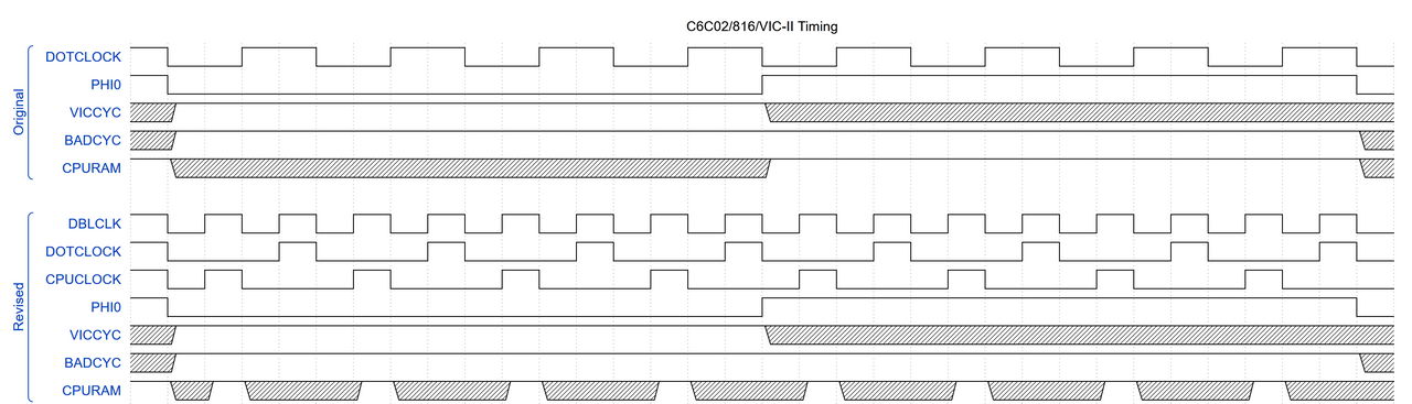
This assumes the VIC-II can handle a cycle width half as wide as it normally sees, but for sake of argument...
As you can see, PHI0 is still 1MHz, and a bad cycle still consumes 100% of it, meaning the entire cycle is not available for the CPU.
(For reference, this timing diagram is from WaveDrom -
https://wavedrom.com/editor.html and the code to create it is:
Code: Select all
{signal: [
  		  	["Original",
           		{name: 'DOTCLOCK',wave: 'hl.h.l.h.l.h.l.h.l.h.l.h.l.h.l.h.l'},
  				{name: 'PHI0',    wave: 'hl...............h...............l'},
  				{name: 'VICCYC',  wave: 'x1...............x................'},
  				{name: 'BADCYC',  wave: 'x1...............................x'},
  				{name: 'CPURAM',  wave: 'hx...............1...............x'},
   		  	],
  				{},
     	     ["Revised",
           		{name: 'DBLCLK',  wave: 'hlhlhlhlhlhlhlhlhlhlhlhlhlhlhlhlhl'},
           		{name: 'DOTCLOCK',wave: 'hl..hl..hl..hl..hl..hl..hl..hl..hl'},
           		{name: 'CPUCLOCK',wave: 'hlhl..hl..hl..hl..hl..hl..hl..hl..'},
  				{name: 'PHI0',    wave: 'hl...............h...............l'},
  				{name: 'VICCYC',  wave: 'x1...............x................'},
  				{name: 'BADCYC',  wave: 'x1...............................x'},
           		{name: 'CPURAM',  wave: '1x1x..1x..1x..1x..1x..1x..1x..1x..'},
		  	]

   		 ],
 config: { hscale: 1 },
 head: 	 { text:'C6C02/816/VIC-II Timing' },
}
An alternative would be to send 8 double speed clocks to the VIC, and then 8 periods of no clock, and let the CPU use that second set of 8 clocks to do work, but I doubt VIC would operate with such an irregular clock, so I think that is a non starter.
The best bet is to throw each address/data line set into a mux with some really fast RAM (if you're planning to run the 65C02 at 8MHz, that means RAM needs to be <125nS, but you need to access it only on the high half cycle, so 62nS or better) and a latch. In the front half of each half cycle, you allow VIC to access, latching the data into a register and then presenting it to the VIC as DATA for the remainder of that half cycle. On the back half of the cycle, let the CPU have the RAM directly. Most of the VIC accesses would go unused, but each device would have total access to RAM (some provision needs to be made for when the CPU needs to talk to the VIC, but to do that, it needs to slow down to 1MHz, and then you're waiting on the VIC anyway:
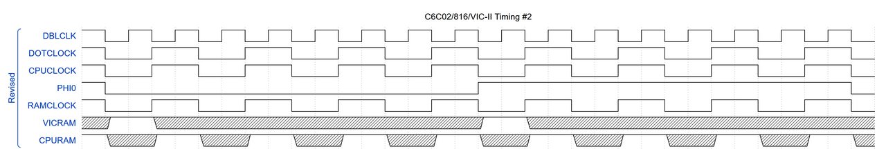
Code: Select all
{signal: [
     	     ["Revised",
           		{name: 'DBLCLK',  wave: 'hlhlhlhlhlhlhlhlhlhlhlhlhlhlhlhlhl'},
           		{name: 'DOTCLOCK',wave: 'hl.h.l.h.l.h.l.h.l.h.l.h.l.h.l.h.l'},
           		{name: 'CPUCLOCK',wave: 'hl.h.l.h.l.h.l.h.l.h.l.h.l.h.l.h.l'},
  				{name: 'PHI0',    wave: 'hl...............h...............l'},
  				{name: 'RAMCLOCK',wave: 'hl.h.l.h.l.h.l.h.l.h.l.h.l.h.l.h.l'},
  				{name: 'VICRAM',  wave: 'x1.x.............1.x..............'},
           		{name: 'CPURAM',  wave: '1x.1.x.1.x.1.x.1.x.1.x.1.x.1.x.1.x'},
		  	]

   		 ],
 config: { hscale: 1 },
 head: 	 { text:'C6C02/816/VIC-II Timing #2' },
}
Realistically, the VIC address lines won't settle down that fast, so you'd need to put the VIC data access about midway through the 1MHz half cycle (but, I didn't feel like updating my diagram, so just imagine it). In any case, that's the best way to use a 1MHz VIC-II and an 8MHz '02/816 and not have to deal with bad cycles.
Jim
Re: Theorizing about interfacing a NMOS VIC-II with a 65cxx
Posted: Fri Aug 07, 2020 5:39 pm
by tokafondo
Another way could be giving VIC-II its own RAM (32K, 64K...) where it would read everything from, and make the CPU access that RAM only to store graphic data, and access a different physical RAM for running code, calculations and so.
The VIC-II would run thinking it is actually halting the CPU, but the CPU wouldn't be being halted, as AEC wouldn't be tied to RDY in the CPU.
But the CPU should be aware of when the VIC-II is reading the VRAM, so it wouldn't try to access it at the same time as it. Could be AEC line of the VIC-II used for such an awareness, instead of halting the CPU?
Re: Theorizing about interfacing a NMOS VIC-II with a 65cxx
Posted: Fri Aug 07, 2020 6:07 pm
by brain
If the CPU tries to access the graphics data when VIC is accessing, it'd have to be halted for the duration of the VIC access time (could be up to 65uS). So, your idea is more prone to stalling. If you mirror the RAM, then reads can be done from other RAM, while writes would still stall.
Jim
Re: Theorizing about interfacing a NMOS VIC-II with a 65cxx
Posted: Fri Aug 07, 2020 8:22 pm
by tokafondo
If the CPU tries to access the graphics data when VIC is accessing, it'd have to be halted for the duration of the VIC access time (could be up to 65uS). So, your idea is more prone to stalling. If you mirror the RAM, then reads can be done from other RAM, while writes would still stall.
Jim
That's why I thought using the AEC pin not for halting the CPU but for signaling: the code that would update the graphics data in VRAM would check throught AEC if access should be allowed.
Every time a read or write to a memory location inside the VRAM would be tried, the first thing to do would be "is AEC active?", and if "Yes", then do a NOP, and ask for AEC status again. When AEC wouln't be active that would mean that the VIC is not accessing the VRAM area, and the access would be allowed. But again, all of this by software, instead of relying on the CPU internal RDY signal.
Would it be safely assumed that a memory access by the VIC lasts half, or a full cycle of PHI0?
Re: Theorizing about interfacing a NMOS VIC-II with a 65cxx
Posted: Fri Aug 07, 2020 10:03 pm
by brain
I understand, and you can do NOP instead of halting the CPU, but the effect is the same (62-65 uS of the CPU waiting). A badline is 62-65 cycles of consecutive double VIC-II accesses, with no RAM time available for the CPU.
Jim
Re: Theorizing about interfacing a NMOS VIC-II with a 65cxx
Posted: Fri Aug 07, 2020 11:22 pm
by tokafondo
I understand, and you can do NOP instead of halting the CPU, but the effect is the same (62-65 uS of the CPU waiting). A badline is 62-65 cycles of consecutive double VIC-II accesses, with no RAM time available for the CPU.
Jim
Well... you are right. Even if the VIC-II have no access to the rest of the RAM, the bus would be shared amongst all the chips in this setup, so the CPU would be waiting for access
any RAM, so...
What about a dual bus? I mean... Electronics experts would tell better, but there must be a way to have the VIC-II to have its own RAM, physically separated from the rest of the system, and the CPU his. But when certain addresses are
touched by the CPU, and the VIC-II is
not accessing those same locations, the
magic would make the CPU access that video-bus, read/write there, and leave out. And I mean, physically leaving out, because the
magic would keep the system-bus and the video-bus apart until needed again, so if the CPU is doing anything else like calculations or reading or writing data from or to ports, or whatever, it would be free to do it while the VIC-II is only keeping busy
its video-bus.
It would be like... the computer having a video card with its own memory.
feasible? doable?
Re: Theorizing about interfacing a NMOS VIC-II with a 65cxx
Posted: Fri Aug 07, 2020 11:37 pm
by brain
Re: Theorizing about interfacing a NMOS VIC-II with a 65cxx
Posted: Sat Aug 08, 2020 2:47 pm
by LeoN
tokafondo, what do You think about
asynchronous dual-port SRAM?
Try use it like
this.
Here you can find them at reasonable prices,
for example.
Re: Theorizing about interfacing a NMOS VIC-II with a 65cxx
Posted: Sun Aug 09, 2020 2:43 pm
by tokafondo
Well, it seems dual port ram could do it... But it seems to be that an address decoder would be still needed, and some sort of PLA-like chip, because of the way the VIC-II work.
Anyway: is a dual port the only solution? It's like, the DPRAM would be the chip that would be managing a dual bus thing... but now I think that there should be a way for the CPU to manage the VIC-II registers, and having this DPRAM solution wouldn't allow the CPU doing that.
There must be something else... Something that allows isolating the VIC-II from the rest of the system when needed, so the CPU have free access to the RAM. Beamracer seems to be doing exactly that.
Re: Theorizing about interfacing a NMOS VIC-II with a 65cxx
Posted: Sun Aug 09, 2020 3:33 pm
by BigEd
In a related discussion over on cbm-hackers, user 'smf' posted a link to this project, which runs a 4MHz 6502 in a C64:
http://wiki.projekt64.filety.pl/doku.ph ... kt64/turbo
via
https://csdb.dk/release/?id=102360
Re: Theorizing about interfacing a NMOS VIC-II with a 65cxx
Posted: Sun Aug 09, 2020 3:51 pm
by 1024MAK
The answer is, how much custom or glue logic do you want to throw at the problem.
There are other systems where various methods have been used to either stop the microprocessor only when it’s accessing the RAM where the video data is located. Or to allow the main microprocessor to continue to execute a program or read/write data during the time that video system is using the RAM where the display data is located.
For the former, having different physical memory chips with tristate buffers to allow the microprocessor to access the RAM chips which hold the video data is possible. When not accessing video RAM, the uP runs at full speed. When it tries to access the video RAM, it’s paused until the video system has a time slot where it does not need access.
Or the video RAM can be completely separate from the microprocessor memory map, with tristate latches used to allow writes to the video RAM only during the time that the video system does not need access. The microprocessor loads up the required address and the data then that is used to access the separate bus. This can even be made to be a FIFO buffer that automatically does the writes without the microprocessor having to sit waiting for access.
But if you are going that far, maybe a better solution would be to produce a new video controller using a FPGA.
Mark
Re: Theorizing about interfacing a NMOS VIC-II with a 65cxx
Posted: Sun Aug 09, 2020 6:50 pm
by tokafondo
Thank you. Yes, the FPGA would be the easy way... And I say easy because it could be designed as desired.
But the VIC-II is not a bad graphics chip. It does what it does nicely, and it has been more than proven the things it can do when programmed properly.
So why not boost it with the capabilities of a faster processor? And that's the talk here. Thanks.
Re: Theorizing about interfacing a NMOS VIC-II with a 65cxx
Posted: Sun Aug 09, 2020 6:53 pm
by brain
Beamracer implements a dual port functionality in the CPLD/FPGA, just like I described initially.
Yes dual port RAM would prevent accessing the VIC registers. You'd have to have a "bypass" that allows the CPU to talk directly to the VIC-II
And, 1024MAK is right. Anything is possible, but it requires lots of glue logic to implement.
Jim
Re: Theorizing about interfacing a NMOS VIC-II with a 65cxx
Posted: Mon Aug 10, 2020 5:11 am
by ttlworks
Don't know if this is helpful, but I now remembered that there had been a
project for running the C64 at 2MHz,
by resorting to a 6502A and SRAM (instead of DRAM).