Starting with my first SBC Project, Plans and Confusions
Posted: Thu Jan 23, 2020 6:22 pm
Hi, this is my first post here on the Forum so please excuse me if i already did anything wrong.
a little bit of background about myself:
I've been into electronics since atleast 5 years, i'm relatively good with ths soldering iron though i never did anything with SMD before.
I got into Retrocomputing and 8 bit hardware a few years ago, and also got my foot in Hardware design and FPGAs.
because i started with the Z80 I'm very used to it's Assembler Syntax and based my early CPU designs on it.
now i got into the 65C02 and 65C816 so the last 2 CPUs i designed were based on those.
I can sort of write software, i used CustomASM to write assemblers for my self made CPUs so i can easily program with them. (i also made an Assembler for the 65C02, but with Z80 Syntax)
but i still need a lot of help when it comes to actually writing something more complex. for example it took me like a weekend to make Tic-Tac-Toe...
but anyways, now to the main post:
I wanted to make a SBC ever since i started with the Z80. but that project never left the Breadboard stage.
Now i want to try again with a but this time skip the Breadboards and just go to a PCB directly.
at first i got the idea of making a SBC with one of my custom CPUs using an FPGA, since FPGAs can run a lot faster and contain multiple circuits (Decoding logic, CPU, Video Chip, etc).
but Ultimately i decided agaist it because for a first time project and first PCB i should choose something much simpler.
The Hardware:
CPU: 1x 65C02 (an obvious choice i think, if possible i'd like to run it at 16, 14 or 10 MHz)
RAM: 2x 32kB SRAM 12ns (i cannot find any other fast RAM as DIP Package)
ROM: 1x 512kB FLASH 70ns (FLASH chips are faster than EEPROMs, and i got a few of these lying around, so ordering smaller ones would be a waste)
UART: 1x FT240X (personally: USB > RS232, these chips handle everything without any external circuitry, USB Protcol, Baudrate, etc... it's just beautiful. plus i can use the USB Connector for Power as well)
Glue Logic: +3x GAL22V10D 4ns max delay (I got like +10 of these and a TL866II+ programmer, so i don't have to deal with regular logic ICs. they should be fast enough for a 65C02 at +10MHz)
Memory Map:
RAM: 0x0000 - 0xDFFF (56kB)
IO: 0xDFF8 - 0xDFFF (8 possible devices, ontop of RAM)
ROM: 0xE000 - 0xFFFF (8kB, also ontop of RAM)
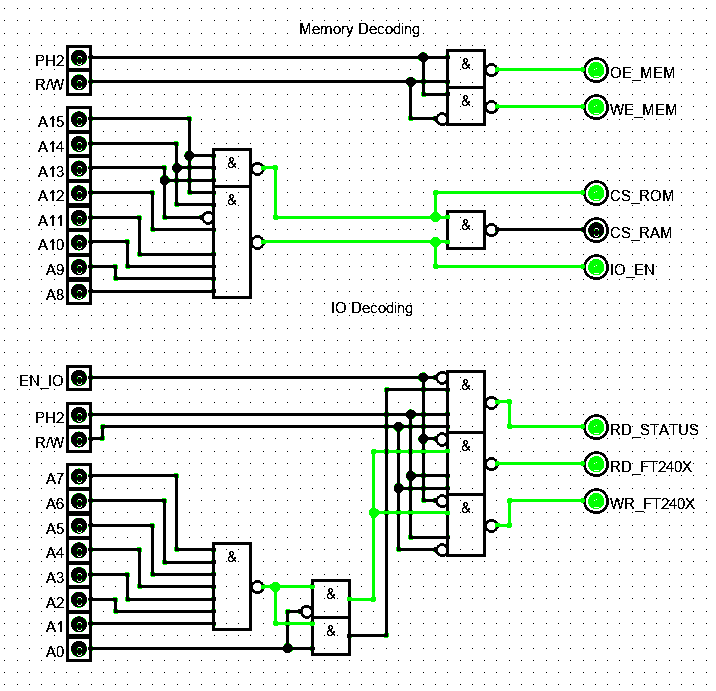
Decoding Logic:
Decoding the Addressess is relatively easy.
If the address is 0b111xxxxxxxxxxxx it's ROM, if it's 0b1101111111111xxx it's IO, and if it's neither it's RAM.
I actually already designed a Logic Circuit for this:
The idea was to split the decoding onto 3 GALs.
the first one for the main Address Decoding, it completely handles the Memory (OE_MEM goes to both ROM and RAM, WE_MEM goes to RAM, the CS' should be obvious)
the second one is for the IO Decoding and handles the FT240X's Access. one thing i noticed about the FT240X is that the datasheet says that it reacts to the falling edge of the WE signal. so i assume i can just constantly pull the WE pin high until the CPU actually writes to it. or should i do it like with RAM but inverted? so the WE is low by default and gets set to high as it writes?
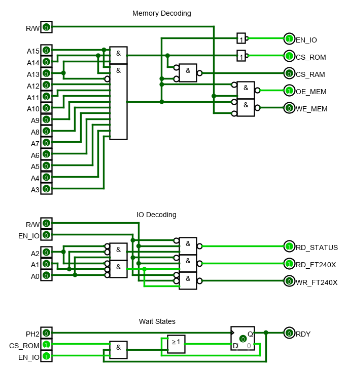
lastly there is the Wait State Circuit i used this post as help to design it. it should activate everytime ROM or IO is accessed.
Lasty, the PCB Design:
I planned on using KiCad for this, i know a bit about it... with the right libraries or custom symbols i should be able to make the Schematic but i'm not sure about the actual PCB design, especailly since i plan on using GALs for the Logic... how does that translate from a Schematic to a PCB?
and why does KiCad have like 10 billion 4 pin Oscillators to choose from? and which is the generic rectangle one?
EDIT: i forgot, it would be amazing if i could have pin headers on the PCB for possible expansion cards or a breadboard. so i can add whatever i want to the system. though it would make the decoding circuitry a lot more complex as the addtional devices could need wait states or use part of the Memory Map so it would need to disable RAM, etc.
so probably not a good idea right now.
so as you can see. my knowledge is kind of all over the place. I always know a few things here and there but never got a complete idea. but hey that's what i'm here for. so that some of you can hopefully help me to get a complete thing done.
I'm sorry if there is Information missing, or something is confusingly written, it took me multiple days to write and re-write this because i'm not very confident about posting stuff. especially when i'm new somewhere.
I will probably edit this multiple times to fix mistakes or add information, but i just want to finally post this and not overthink it too much.
a little bit of background about myself:
I've been into electronics since atleast 5 years, i'm relatively good with ths soldering iron though i never did anything with SMD before.
I got into Retrocomputing and 8 bit hardware a few years ago, and also got my foot in Hardware design and FPGAs.
because i started with the Z80 I'm very used to it's Assembler Syntax and based my early CPU designs on it.
now i got into the 65C02 and 65C816 so the last 2 CPUs i designed were based on those.
I can sort of write software, i used CustomASM to write assemblers for my self made CPUs so i can easily program with them. (i also made an Assembler for the 65C02, but with Z80 Syntax)
but i still need a lot of help when it comes to actually writing something more complex. for example it took me like a weekend to make Tic-Tac-Toe...
but anyways, now to the main post:
I wanted to make a SBC ever since i started with the Z80. but that project never left the Breadboard stage.
Now i want to try again with a but this time skip the Breadboards and just go to a PCB directly.
at first i got the idea of making a SBC with one of my custom CPUs using an FPGA, since FPGAs can run a lot faster and contain multiple circuits (Decoding logic, CPU, Video Chip, etc).
but Ultimately i decided agaist it because for a first time project and first PCB i should choose something much simpler.
The Hardware:
CPU: 1x 65C02 (an obvious choice i think, if possible i'd like to run it at 16, 14 or 10 MHz)
RAM: 2x 32kB SRAM 12ns (i cannot find any other fast RAM as DIP Package)
ROM: 1x 512kB FLASH 70ns (FLASH chips are faster than EEPROMs, and i got a few of these lying around, so ordering smaller ones would be a waste)
UART: 1x FT240X (personally: USB > RS232, these chips handle everything without any external circuitry, USB Protcol, Baudrate, etc... it's just beautiful. plus i can use the USB Connector for Power as well)
Glue Logic: +3x GAL22V10D 4ns max delay (I got like +10 of these and a TL866II+ programmer, so i don't have to deal with regular logic ICs. they should be fast enough for a 65C02 at +10MHz)
Memory Map:
RAM: 0x0000 - 0xDFFF (56kB)
IO: 0xDFF8 - 0xDFFF (8 possible devices, ontop of RAM)
ROM: 0xE000 - 0xFFFF (8kB, also ontop of RAM)
Decoding Logic:
Decoding the Addressess is relatively easy.
If the address is 0b111xxxxxxxxxxxx it's ROM, if it's 0b1101111111111xxx it's IO, and if it's neither it's RAM.
I actually already designed a Logic Circuit for this:
The idea was to split the decoding onto 3 GALs.
the first one for the main Address Decoding, it completely handles the Memory (OE_MEM goes to both ROM and RAM, WE_MEM goes to RAM, the CS' should be obvious)
the second one is for the IO Decoding and handles the FT240X's Access. one thing i noticed about the FT240X is that the datasheet says that it reacts to the falling edge of the WE signal. so i assume i can just constantly pull the WE pin high until the CPU actually writes to it. or should i do it like with RAM but inverted? so the WE is low by default and gets set to high as it writes?
lastly there is the Wait State Circuit i used this post as help to design it. it should activate everytime ROM or IO is accessed.
Lasty, the PCB Design:
I planned on using KiCad for this, i know a bit about it... with the right libraries or custom symbols i should be able to make the Schematic but i'm not sure about the actual PCB design, especailly since i plan on using GALs for the Logic... how does that translate from a Schematic to a PCB?
and why does KiCad have like 10 billion 4 pin Oscillators to choose from? and which is the generic rectangle one?
EDIT: i forgot, it would be amazing if i could have pin headers on the PCB for possible expansion cards or a breadboard. so i can add whatever i want to the system. though it would make the decoding circuitry a lot more complex as the addtional devices could need wait states or use part of the Memory Map so it would need to disable RAM, etc.
so probably not a good idea right now.
so as you can see. my knowledge is kind of all over the place. I always know a few things here and there but never got a complete idea. but hey that's what i'm here for. so that some of you can hopefully help me to get a complete thing done.
I'm sorry if there is Information missing, or something is confusingly written, it took me multiple days to write and re-write this because i'm not very confident about posting stuff. especially when i'm new somewhere.
I will probably edit this multiple times to fix mistakes or add information, but i just want to finally post this and not overthink it too much.