Page 1 of 4

Experimental TTL implementation of the 6522

Posted: Mon Mar 04, 2019 4:42 pm
by ttlworks
For supporting a project which aims at building a TTL implementation of the 6526,
I dug out my old schematics for an experimental 6522 TTL implementation, the X22.

Because the most recent version of Eagle can't open Eagle 3.55 files anymore, I converted them to *.png.

Edit:
The thread became a bit longer than expected, also featuring:
6521, 6523, 6532, 6545, 6551\6850.

;---

The design was experimental and partially untested,
I'm not sure if the timers were cycle exact,
and if you try to make use of these echematics,
please take them with a grain of salt and try to build things a bit different from them.

It seemed to have worked with a Rockwell R65C02-2 running at 4MHz.
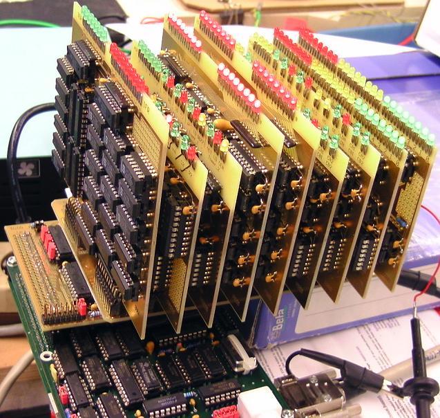
Image

Test setup:

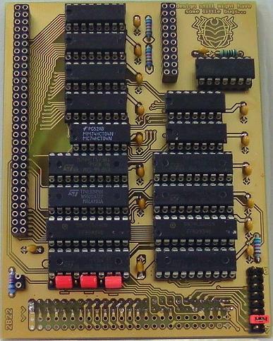
Bottom: my DRC2 SBC, which is supposed to be compatible to the SBC-2.

2B22 bus interface is plugged into DRC2.
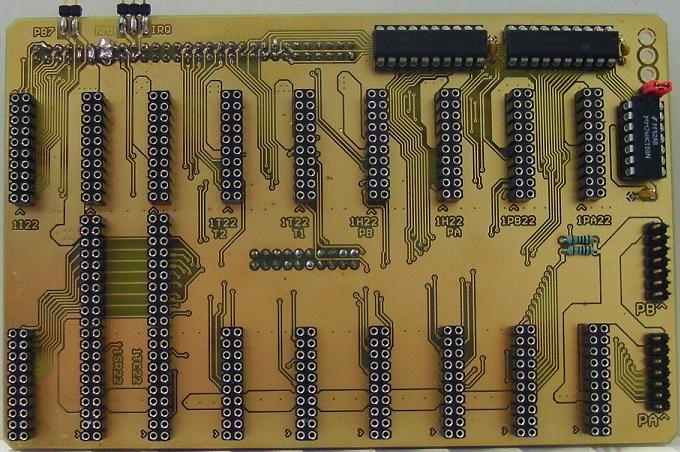
X22 backplane is plugged into the 2B22 bus interface.

Plugged into the X22 backplane, we have:
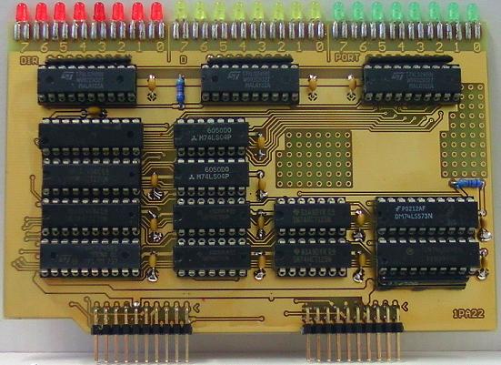
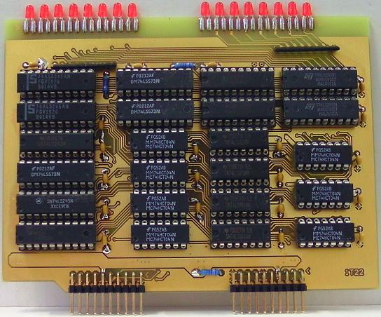
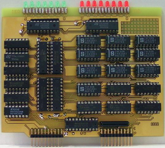
1* 1PA22, Port A module
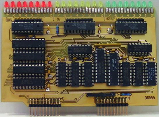
1* 1PB22, Port B module
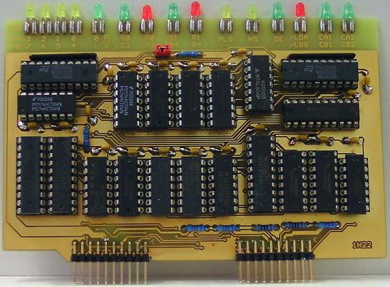
2* 1H22, handshake module
2* 1T22, timer module
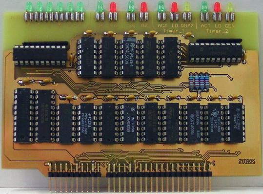
1* 1TC22, timer control module
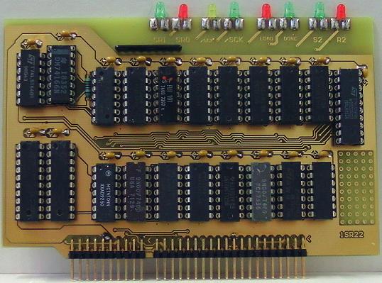
1* 1SR22, shift register module
1* 1I22, interrupt module

Re: Experimental TTL implementation of the 6522

Posted: Mon Mar 04, 2019 4:48 pm
by ttlworks
First the bus interface 2B22, which also had been used for other projects (don't get confused).
The bus interface was plugged between the computer and the X22 backplane.

Image

It assumes that the address bus is stable when PHI2 goes HIGH,
same thing for the data bus during write cycles...
what, of course, isn't the case in a C64 when CPU and VIC-II are sharing the bus.

For a TTL implementation of the 6526, please build things different, sorry.
2b22_1.png
2b22_2.png
2b22_3.png
2b22_3.png

Re: Experimental TTL implementation of the 6522

Posted: Mon Mar 04, 2019 4:51 pm
by ttlworks
Now for the X22 backplane:

Image
1x22_1.png
1x22_2.png
1x22_3.png
1x22_4.png
1x22_5.png

Re: Experimental TTL implementation of the 6522

Posted: Mon Mar 04, 2019 4:54 pm
by ttlworks
Now for port A, which has open collector outputs: 1pa22

Image
1pa22_1.png
1pa22_2.png
1pa22_3.png
1pa22_4.png

Re: Experimental TTL implementation of the 6522

Posted: Mon Mar 04, 2019 4:57 pm
by ttlworks
Port B has three state outputs: 1pb22

Image
1pb22_1.png
1pb22_2.png
1pb22_3.png
1pb22_4.png
1pb22_5.png

Re: Experimental TTL implementation of the 6522

Posted: Mon Mar 04, 2019 5:00 pm
by ttlworks
Handshake PCB: 1h22, two such PCBs required.

One PCB for port A, another (identical) PCB for port B, but jumper settings for both PCBs are different.

Image
1h22_1.png
1h22_2.png
1h22_3.png
1h22_4.png
1h22_5.png

Re: Experimental TTL implementation of the 6522

Posted: Mon Mar 04, 2019 5:01 pm
by ttlworks
1h22_6.png
1h22_7.png

Re: Experimental TTL implementation of the 6522

Posted: Mon Mar 04, 2019 5:07 pm
by ttlworks
16 Bit timer modules: 1t22, two (nearly) identical PCBs required.

Image

Some chips are not used on one of the PCBs, but having all of the chips plugged into both PCBs does no harm.

Since getting hands on down_counters turned out to be difficult,
I just had used up_counters while puttting 7404 inverters into the counter inputs and outputs...
to make them up_counters look like down_counters to the CPU.

Again: I'm not sure if timer overflow etc. is cycle exact, you better check !
1t22_1.png
1t22_2.png
1t22_3.png
1t22_4.png
1t22_5.png

Re: Experimental TTL implementation of the 6522

Posted: Mon Mar 04, 2019 5:10 pm
by ttlworks
Since we have two timers,
we also have a timer control PCB for the two timers: 1tc22

Image
1tc22_1.png
1tc22_2.png
1tc22_3.png
1tc22_4.png
1tc22_5.png

Re: Experimental TTL implementation of the 6522

Posted: Mon Mar 04, 2019 5:13 pm
by ttlworks
Now for that shift register PCB with all these odd operating modes, which gave me quite a headache: 1sr22

Image
1sr22_1.png
1sr22_2.png
1sr22_3.png
1sr22_4.png
1sr22_5.png

Re: Experimental TTL implementation of the 6522

Posted: Mon Mar 04, 2019 5:17 pm
by ttlworks
Now for the last part, the interrupts: 1i22

Image

The 100nF capacitors are hidden below the IC sockets.
Again I'm not sure if things are cycle exact, and you better check before trying to rebuild it.
1i22_1.png
1i22_2.png
1i22_3.png
1i22_4.png
1i22_5.png

Re: Experimental TTL implementation of the 6522

Posted: Mon Mar 04, 2019 5:19 pm
by ttlworks
1i22_6.png
...and I think that's the whole set of schematics.

Again: it was experimental, not everything was tested, you probably would have to build things a bit different,
all the hardware went scrapped years ago, and I don't remember much of all the details after all these years.

Good luck.

Re: Experimental TTL implementation of the 6522

Posted: Mon Mar 04, 2019 5:27 pm
by ttlworks
(Muckraking around in a dusty drawer)
But wait: there is more.

Years ago I also did some paperwork for a 6522 TTL implementation, aiming at 20MHz.

Untested stuff, never built, a mere paper design, contains some odd tricks,
better analyze them schematics carefully before trying to put any of that circuitry into use.
...and better check, if timers and interrupts are cycle exact.

Here we go.
6522_1.png
6522_2.png
6522_3.png
6522_4.png
Address has to be stable before the _falling_ edge of PHI2,
same thing for data during write cycles.
IIRC there also is a trick for preventing ghost interrupts.

Again: good luck... and now: get off my lawn.

Re: Experimental TTL implementation of the 6522

Posted: Mon Mar 04, 2019 6:36 pm
by whartung
Great work ttlworks!

Re: Experimental TTL implementation of the 6522

Posted: Mon Mar 04, 2019 8:18 pm
by GARTHWILSON
Your construction is always amazing. Quite the eye candy!