Understanding the SID
Posted: Wed Jun 08, 2016 4:06 pm
This is my attempt at reverse-engineering (parts of) the SID chip from the schematics available at http://oms.wmhost.com/misc/. I'm not a hardware guy so support from experts is needed  .
.
The results of this research wil be used to improve the open-source reSID emulation and will be put online at the libsidplayfp project wiki.
Let's start with the noise generator. As already known the noise waveform is generated taking the output of eight selected bits from a 23 bit Fibonacci LFSR (there are actually 24 bits on chip but the last one is unused). The register is clocked when bit 19 of the oscillator goes high and has taps at 17 and 22. The register can be reset using the test bit.
Each bit is formed by two inverters feeding each other through the gates c1 and c2, while the gate LC controls the shifting. The output from bits 0, 2, 5, 9, 11, 14, 18 and 20 is sent to the waveform selector. Here's the first two bits from the vectorized IC and the transistor scheme for a single bit:
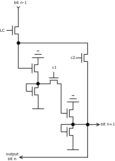
So the first question is:
when combining the noise with other waveforms the output bits may be driven low locking up the LFSR at zero. My understanding is that this happens only when when the gate LC is opened, during shifting or when the test bit is set, as the output bits are then feeded into the next ones (this seems to be confirmed by empirical tests, see VICE's bug 746). Is this correct? In other words, is it safe to assume that when a bit output (e.g. Noise 0 in the above picture) is grounded the bit itself is not written into?
The results of this research wil be used to improve the open-source reSID emulation and will be put online at the libsidplayfp project wiki.
Let's start with the noise generator. As already known the noise waveform is generated taking the output of eight selected bits from a 23 bit Fibonacci LFSR (there are actually 24 bits on chip but the last one is unused). The register is clocked when bit 19 of the oscillator goes high and has taps at 17 and 22. The register can be reset using the test bit.
Each bit is formed by two inverters feeding each other through the gates c1 and c2, while the gate LC controls the shifting. The output from bits 0, 2, 5, 9, 11, 14, 18 and 20 is sent to the waveform selector. Here's the first two bits from the vectorized IC and the transistor scheme for a single bit:
So the first question is:
when combining the noise with other waveforms the output bits may be driven low locking up the LFSR at zero. My understanding is that this happens only when when the gate LC is opened, during shifting or when the test bit is set, as the output bits are then feeded into the next ones (this seems to be confirmed by empirical tests, see VICE's bug 746). Is this correct? In other words, is it safe to assume that when a bit output (e.g. Noise 0 in the above picture) is grounded the bit itself is not written into?