A couple assorted questions about internal structure of 6502
Posted: Wed Nov 11, 2015 2:20 pm
Hello everyone!
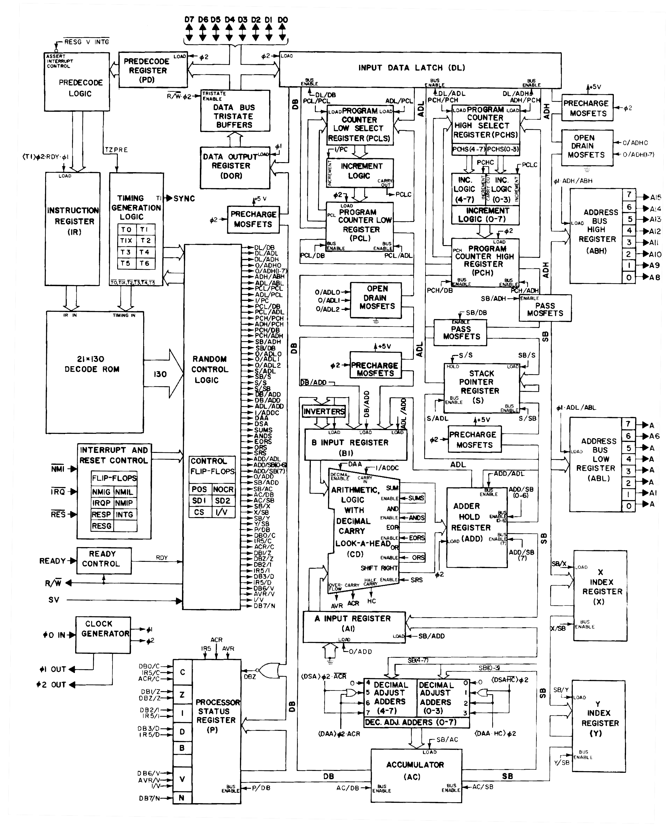
I have been poring over the block diagram of the 6502 and I think I have a general understanding of things, but there are a few questions I still have:
(1) First of all, the various buses that run throughout the processor. I know that the labels on them were not given by the designer so they're kink of arbitrary, but they mostly seem to have names that makes sense: DB is used to transfer data to/from the data bus pins, ADL/ADH connect to the two pieces of the address bus. But SB left me a bit confused. I've decided that because it's connected to the output of the ALU maybe it means sum bus?
(2) Precharge and open drain mosfets. What does that mean? Do they serve a logical function, or are they only involved in providing power and ground (or something like that)?
(3) The pass mosfets between SB and DB (and also SB and ADH and maybe another one I missed), I think I understand. They are not transferring any data between the buses, but joining the buses together so that (while the pass mosfet is enabled) the two buses always have the same value, and will be required to only have one device between the two buses that is enabled?
(4) Is there any documentation on the random control logic? I've studied the instruction decoder, but this only gives arbitrary names to the 130 lines of the bus that connects it to the random control logic. I haven't been able to find any information on how the random control logic converts the 130 inputs to the 50 or so control lines.
(5) Another user on this forum gave a really good cycle by cycle breakdown of what happens when the processor executes LDA $4321. I understand how the clock signal is turned into a two-phase clock, so start and end of the cycle in BigEd's explanation, I assume, refer to phi-1 and phi-2. How does the processor synchronize with the "middle" of the cycle?
Thank you very much for any help