Page 1 of 1

Proof reading memory map

Posted: Mon Oct 12, 2015 4:49 am
by yvibod
Hello! If you guys could help me go through my memory decoding scheme to make sure I haven't done anything wrong that would be greatly appreciated :D
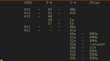
Chips:
3 - 2k ROM
3 - 2k RAM
1 - 6522 VIA
1 - 74LS139 2 to 4 decoder (two on the dip)
1 - 74LS138 3 to 8 decoder

Goal is to divide the address space in 8 chunks of 8k, and the first and last chunks into 4 2k each. The 3-8 decoder will enable the adequate side of the 2-4 decoder through it's enable lines (here marked Ea and Eb) which will
then enable the appropriate chip.

Image

Intended memory map:

Image

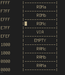
Sorry if I'm a little too hard to understand, this is my first attempt at this.

Re: Proof reading memory map

Posted: Mon Oct 12, 2015 5:43 am
by mkl0815
Hello,

it would be good to have a schematic and the types of your ROM and RAM chips. Some of them have more then one chipselect line and this could make address decoding simpler.

Mario.

Re: Proof reading memory map

Posted: Mon Oct 12, 2015 2:17 pm
by 8BIT
I believe this is what yvibod is trying to describe
sch.jpg

Re: Proof reading memory map

Posted: Mon Oct 12, 2015 4:09 pm
by yvibod
8BIT wrote:
I believe this is what yvibod is trying to describe
sch.jpg
Wow, thank you for taking the time!

Here are the schematics on the chips:

ROM:
Image
Image

RAM:
Image
Image

Re: Proof reading memory map

Posted: Mon Oct 12, 2015 7:04 pm
by 8BIT
Happy to help.

Re: Proof reading memory map

Posted: Tue Oct 13, 2015 6:49 pm
by Dr Jefyll
yvibod wrote:
this is my first attempt at this.
Looks like you've got a good grasp of the subject, yvibod. :) But it may be your circuit is more complex than necessary.
yvibod wrote:
Goal is to divide the address space in 8 chunks of 8k, and the first and last chunks into 4 2k each.
And your circuit maps the six 8k chunks in the middle to nothing. But is it an actual requirement to have nothing there (so there's plenty of room for future expansion perhaps)? If not, there's an alternative arrangement (below) which omits the '139 decoder and uses just a '138. Apologies, Daryl, for hacking your diagram! :D
sch mod-A.jpg
It's A13, A12 and A11 that drive the '138 inputs, and that means each of the '138 outputs will span a 2K range. But A15 and A14 are "no connect" -- they are ignored. The resulting memory map looks roughly like this. (I didn't draw the whole thing.)
map mod-A.png
map mod-A.png (3.38 KiB) Viewed 1656 times
Notice that the 0 - $3FFF region is identical to the $4000 to $7FFF region. Although I didn't draw the whole thing, $8000-$BFFF is the also the same, and $C000-$FFFF too. It's the result of ignoring A15 and A14.

From a coding perspective, LDA $0000 (for example) has the same effect as LDA $4000 or LDA $8000 or LDA $C000. And LDA 1 is the same as $4001 and $8001 and $C001, and so on.

It's harmless to have all those aliases. The only drawback is if you want to add more devices in future. There's only a 2K space left available (at $1800 aka $5800 aka $9800 aka $D800).

Edit:
yvibod wrote:
Here are the schematics on the chips:
Re: the 6522 you'll need to connect the '138 output to 6522 /CS (pin 23), and tie the 6522 CS input (pin 24) high.

cheers,
Jeff

ps- here at 6502.org you can include images as attachments to your post. You'll find that more convenient than putting the images on a third-party site, and it also ensures the images will remain permanently available.

Re: Proof reading memory map

Posted: Wed Oct 14, 2015 11:56 pm
by yvibod
Dr Jefyll wrote:
yvibod wrote:
this is my first attempt at this.
Looks like you've got a good grasp of the subject, yvibod. :) But it may be your circuit is more complex than necessary.
yvibod wrote:
Goal is to divide the address space in 8 chunks of 8k, and the first and last chunks into 4 2k each.
And your circuit maps the six 8k chunks in the middle to nothing. But is it an actual requirement to have nothing there (so there's plenty of room for future expansion perhaps)? If not, there's an alternative arrangement (below) which omits the '139 decoder and uses just a '138. Apologies, Daryl, for hacking your diagram! :D
sch mod-A.jpg
It's A13, A12 and A11 that drive the '138 inputs, and that means each of the '138 outputs will span a 2K range. But A15 and A14 are "no connect" -- they are ignored. The resulting memory map looks roughly like this. (I didn't draw the whole thing.)
map mod-A.png
Notice that the 0 - $3FFF region is identical to the $4000 to $7FFF region. Although I didn't draw the whole thing, $8000-$BFFF is the also the same, and $C000-$FFFF too. It's the result of ignoring A15 and A14.

From a coding perspective, LDA $0000 (for example) has the same effect as LDA $4000 or LDA $8000 or LDA $C000. And LDA 1 is the same as $4001 and $8001 and $C001, and so on.

It's harmless to have all those aliases. The only drawback is if you want to add more devices in future. There's only a 2K space left available (at $1800 aka $5800 aka $9800 aka $D800).

Edit:
yvibod wrote:
Here are the schematics on the chips:
Re: the 6522 you'll need to connect the '138 output to 6522 /CS (pin 23), and tie the 6522 CS input (pin 24) high.

cheers,
Jeff

ps- here at 6502.org you can include images as attachments to your post. You'll find that more convenient than putting the images on a third-party site, and it also ensures the images will remain permanently available.
That's way simpler! Specially because I'm going to hand solder the thing this is very cool, Thank you for taking the time!

Re: Proof reading memory map

Posted: Thu Oct 15, 2015 3:58 am
by Dr Jefyll
You're welcome. Just recently we were discussing something similar, BTW -- a project using 6503, which can't connect to the upper address pins because the 6503 doesn't have any upper address pins!

Good luck, and keep us posted.