Page 1 of 3
My MARC-1 SBC
Posted: Mon Oct 28, 2013 7:02 pm
by lordbubsy
This is my MARC-1 SBC.
With the PCB layout I started over three times. But I think I’ve got it right now.
It’s pretty simple in address decoding and features. Only an ACIA for I/O.
This is mainly for experimenting and interfacing with the breadboard and will replace my current prototype.
The ATtiny delivers a clock of 3,6864 MHz. This is divided to 1,8432 MHz. for the ACIA and 0,9216 MHz. for PHI2. With a jumper, PHI2 can also be set to 1,8432 MHz.
There are buttons for reset, CPU stop and single instruction.
Code: Select all
Memory Map:

0000-BFFF	RAM
BF00-BFFF	I/O
C000-FFFF	ROM

BF30-BF33	ACIA
Re: My MARC-1 SBC
Posted: Mon Oct 28, 2013 7:08 pm
by Arlet
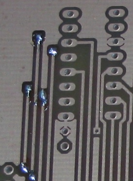
It looks like some vias are really close together. Did you run a design rule check ?
Re: My MARC-1 SBC
Posted: Mon Oct 28, 2013 9:23 pm
by lordbubsy
Hi Arlet,
Did you run a design rule check ?
I’ve used EAGLE’s default design rules, it only gives me some errors with drill sizes of the vias. Do you have any suggestions?
BTW. I used the technique you suggested to apply two polygon layers and assigned them to one level. Before there were 42 air wires, and after there were only 4 left.
Could I use smaller trace width’s for home etching, now I use 0.016”. and for power 0.024”?
Re: My MARC-1 SBC
Posted: Mon Oct 28, 2013 9:52 pm
by Arlet
I was looking at these 3 vias in the middle. What's the space between them ?
Also, some vias can be easily avoided, like the two on the left, by letting the red trace go horizontal for a little bit.
Re: My MARC-1 SBC
Posted: Mon Oct 28, 2013 10:56 pm
by lordbubsy
I was looking at these 3 vias in the middle. What's the space between them ?
It’s 0.01”. I made some room between them.
Also, some vias can be easily avoided, like the two on the left, by letting the red trace go horizontal for a little bit.
Can I reach the upper side for soldering on the sockets? If so, there could be a lot more vias omitted.
Re: My MARC-1 SBC
Posted: Tue Oct 29, 2013 6:48 am
by Arlet
Can I reach the upper side for soldering on the sockets? If so, there could be a lot more vias omitted.
Ah, I didn't think about the fact you were going to etch these yourself and don't have plated through hole. I don't know about sockets, but if you solder the IC in without a socket, it's much easier to reach the top side. For cheap ICs that may be a good option.
If you get some sockets now, you can practice soldering the top side on a piece of perfboard, and see if its possible. Or maybe somebody else has more experience with sockets and can tell if there are suitable ones that can be soldered on the top.
Re: My MARC-1 SBC
Posted: Fri Nov 01, 2013 9:29 am
by lordbubsy
While etching my board, a topic showed up which just fits in here!
viewtopic.php?f=4&t=2760
Arlet, your new Sandbox design looks so clean and easy, I know it’s not...
I’m glad with your advice, it just pushed me over the edge. Here is a photo shoot of the results:
I use a technique described here:
http://thomaspfeifer.net/platinen_aetzen.htm
It’s in German, but I have some similar links in English.
http://www.riccibitti.com/pcb/pcb.htm
http://fullnet.com/~tomg/gooteepc.htm
http://www.dr-lex.be/hardware/tonertransfer.html
The paper I use is from an electronics catalog. I print the bottom layer normal and the top layer mirrored.
Then I glue those two sheets together with one side open like a pocket.
This way I can slide the double sided print in. For melting the toner onto the copper I use a hacked laminator. It regulates at a temperature of ca. 200 deg. Celsius. And heats at both sides simultaneously.
The vias I drill with 0,5mm. I keep the vias at open places to be able to solder a wire through it. Also when I can reach the upper side of the solder pad, I can use it as a via.
Re: My MARC-1 SBC
Posted: Fri Nov 01, 2013 9:34 am
by lordbubsy
There are over 100 vias and over 300 pads, so I'm occupied.

- CRW_0023b.jpg (37.3 KiB) Viewed 1681 times
It has a fairly high success rate. The only flaws are when the copper isn’t clean enough or when the printer has little drop outs.
- CRW_0024b.jpg (3.07 KiB) Viewed 1681 times
Re: My MARC-1 SBC
Posted: Fri Nov 01, 2013 9:40 am
by Arlet
Looks nice.
Re: My MARC-1 SBC
Posted: Fri Nov 01, 2013 1:07 pm
by Aslak3
Looks amazing. I couldn't dream of doing a homemade PCB of that good a quality and have to get mine made in China. Looking forward to seeing the board all populated with parts.
Re: My MARC-1 SBC
Posted: Fri Nov 01, 2013 6:42 pm
by GARTHWILSON
That's definitely the best home board-etching job I've ever seen.
Re: My MARC-1 SBC
Posted: Sat Nov 02, 2013 8:31 am
by lordbubsy
Thanks for the compliments!
However, soldering the true holes is more work than I thought.
Re: My MARC-1 SBC
Posted: Thu Nov 07, 2013 8:58 am
by lordbubsy
Phew, after some days I finished soldering. Unfortunately, Atmel decided to update their Atmel Studio, and my AVRISP-mkII Clone stopped working.
Here is a picture of the result. What’s not pretty is that the copper already begins to corrode.
Re: My MARC-1 SBC
Posted: Thu Nov 07, 2013 4:58 pm
by BigDumbDinosaur
Phew, after some days I finished soldering. Unfortunately, Atmel decided to update their Atmel Studio, and my AVRISP-mkII Clone stopped working.
Here is a picture of the result. What’s not pretty is that the copper already begins to corrode.
024.jpg
Nice looking board. Just use some
Brasso on it and it'll stay shiny.

Re: My MARC-1 SBC
Posted: Thu Nov 07, 2013 5:02 pm
by BigDumbDinosaur
Phew, after some days I finished soldering. Unfortunately, Atmel decided to update their Atmel Studio, and my AVRISP-mkII Clone stopped working.
Here is a picture of the result. What’s not pretty is that the copper already begins to corrode.
024.jpg
BTW, I don't see a bypass capacitor near the EPROM. An EPROM generates a large transient when /OE is asserted.
Something else to consider is that fill planes (aka ground pours) are detrimental to high speed digital circuits.