What does the PLA do in order to resolve instructions
Posted: Tue Oct 22, 2013 9:06 am
I have read a bit on how the 6502 processes instructions but im still a bit confused. From a diagram of a normal pla there is an input with a normal line and an inversion of that same line, and there are lines of the array attached to nothing, then those lines lead to the nor section which go down into the output. 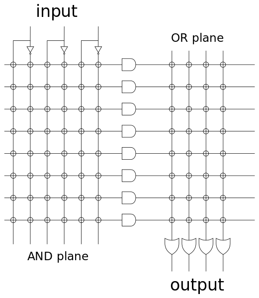
What is the purpose of the inputs and the outputs? I saw that it fires instructions based on timing, but I don't know where that goes in on that schematic. Im attempting to better understand processors and this is a bit confusing to me. I've looked at simulations and i've come up with what I THINK is going on but this might be something different.
So there might be triggers for parts of the cpu, like (Accumulator INPUT) (Accumulator OUTPUT) (X input) (X output) (Load) (Store) etc etc..
And STA might trigger Store, and A, which will select A to dump it's data into the register bus, where the store circuit will pick that up and send it to whatever address is in the argument registers. (example, STA $0D00) would trigger Store, and A. LDA will trigger Load and A, which will pull the data from the address in the argument registers into the register bus and only A will pick that up and lock on the next clock cycle.
I'm aiming to build a very simplified processor from relays or transistors as a project. Instead of being 8 bit it will be 4 bit, the addresses will be 1 byte, which will give me enough room to do very basic functions, allow 16 different instructions. From there i might expand but all in all I'm just trying to learn. Thanks for your help.