Page 1 of 6
6502 Sandbox
Posted: Fri Feb 22, 2013 10:45 am
by Arlet
Inspired by
enso's 6502 playground, I decided to make something similar myself. The attached pictures are for the first prototype, which has a Spartan-6 FPGA, a 6502 or 65816 in PLCC socket, and an 128kB SRAM device. For I/O there's a simple LED, a UART, and a 16 pin header. Just like in enso's project, all 6502 signals are fed into the FPGA, which sits between the 6502 and the rest of the world. This version is just a prototype to test the concept. I'm planning to make a second version on a slightly bigger board with some more interesting I/O capabilities, such as video, audio and USB. I'm using a SPI serial flash for the FPGA configuration, with the serial pins also brought out to a header. This should allow update of the FPGA contents for people without access to JTAG pods.
Re: 6502 Sandbox
Posted: Fri Feb 22, 2013 11:51 am
by SimonJ5
Very interesting - especially with the extended IO options. I like the idea of the 'easily' solderable pins although I'll need to get some new glasses for the FPGA!
Simon
Re: 6502 Sandbox
Posted: Fri Feb 22, 2013 12:01 pm
by ElEctric_EyE
Is it a 4-layer board?
How do you have the 3.3V, 2.5V & 1.2V voltages arranged for the FPGA?
No doubt the 6502 and 65816 will be operated at 3.3V?
Re: 6502 Sandbox
Posted: Fri Feb 22, 2013 12:32 pm
by Arlet
If there's interest, I can make a batch using reflow soldering, and offer them for sale at cost + shipping. The only problem is that everybody will have their own ideal feature set, and it's impossible to satisfy them all

The I/O capabilities of the FPGA are limited, so after adding a video bus, there won't be many pins left for fancy stuff.
For video, my plan is to bring back the CS4954 from
this project, running on
this hardware, but use the RGB/YUV outputs instead of the composite video. I know it's not high res VGA, but with an 8 bit 6502, the resources are limited anyway. Also, I'm more interested in retro than high performance (for high performance, I'd pick an ARM instead). For audio support, I'm thinking about the MAX5556 stereo DAC with I2S interface. The USB port is intended to work as a USB host, for support of a keyboard, or perhaps a memory stick. My plan was to have the FPGA talk directly to the USB devices through 2 IO pins, limiting this to full-speed only.
Re: 6502 Sandbox
Posted: Fri Feb 22, 2013 12:45 pm
by Arlet
It's a 2 layer board. What you see on the pictures, is what you get. The solid copper areas on top/bottom are ground planes. I'm only using 3.3V and 1.2V. Since VCCaux is also 3.3V, there's no 2.5V net on the board. This also means the 6502 runs at 3.3V. There are no level shifters, and I'm assuming a modern WDC device.
For power distribution, see close up image. There are 2 rings underneath the FPGA. The outer ring is 3.3V, the inner ring is 1.2V. There's a SOT-223 1.2V regulator in the middle, and bypass caps all along both rings. There's one capacitor per power pin, and at least one via near every ground pin connecting to both ground planes. There's a couple 10 uF caps, and a bunch of 100 nF ones.
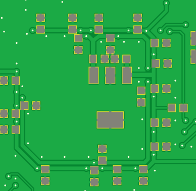
- power.png (30.47 KiB) Viewed 3988 times
Re: 6502 Sandbox
Posted: Sat Feb 23, 2013 12:15 am
by ElEctric_EyE
With that CS4954 video IC, it still needs 2 bytes per pixel I believe. Why not just use a good grade 16-bit RGB videoDAC and make the 8-16bit interface and have a possibility for decent resolution?
Re: 6502 Sandbox
Posted: Sat Feb 23, 2013 6:50 am
by Arlet
Yes, it needs 2(*) bytes per pixel, but it only has an 8 bit bus, so it saves a bunch of wires, while still allowing the full color range. And with the external 6502, I'm really short on IOs. After hooking up the CS4954, I only have about 13 pins left (I may be able to reuse some), and I still need to do audio and USB at least. Also, keep in mind there's an old fashioned 8 bit 6502 on there, running at a modest 8 MHz, with only 128kB of SRAM. Even a plain bitmapped 8 bit VGA-type resolution needs 640*480 = 307200 bytes. That's more than twice the size of my SRAM, and the SRAM is twice is as big as the entire 6502 address space.
Edit: (*) note that it needs 2 bytes per pixel, but it's more accurately described as 4 bytes per 2 pixels, where the brightness is 8 bits per pixel, and color information is 16 bits shared between 2 adjacent pixels.
Re: 6502 Sandbox
Posted: Mon Feb 25, 2013 9:01 am
by Arlet
(copied from other thread)
I like Arlet's decision to use serial EEPROM and offer an SPI programming interface: it means that in principle anyone could put together a bit-banging programmer to turn the populated board into a functioning board, or indeed update the FPGA if needed. It's also true that helpful people could provide pre-programmed EEPROMS at a modest price, which opens up FPGA core-based systems to more people - they can use FPGAs without getting involved in the mechanics.
In fact, the SPI programming interface is also accessible through the FPGA by redefining the configuration pins as user I/O. So once the system is working, the FPGA can be updated by a program running on the 6502, without requiring external hardware. Of course, the user must be careful to send the correct bit file, and not interrupt the power: if the board is restarted with a bad image, the 6502 won't run anymore, and external SPI programming is required to restore it.
Re: 6502 Sandbox
Posted: Mon Feb 25, 2013 9:49 am
by BigEd
This is a very nice feature to allow field upgrades with no tooling!
BTW, I see you bring out a few interfaces off the board: is the 16-pin header pure general purpose I/O? Is there any particular meaning to D, C, S, Q on the SPI connector?
Cheers
Ed
Re: 6502 Sandbox
Posted: Mon Feb 25, 2013 10:15 am
by Arlet
Yes, the 16 pin header is all I/O. As soon as I ordered the PCBs, I realised I forgot to add some ground/vcc pins, but they can be grabbed from the JTAG connector, so it's not a show stopper. The pin header is only a temporary feature for prototyping. In the final version, I'll probably use up nearly all free I/O pins on the FPGA. One option to free more I/O pins is to follow the Propeller board idea, with only a single data/address bus, shared between 6502, SRAM and FPGA. This would save quite a few I/Os, but would reduce flexibility. My goal with this first board is to try out the concept, and help decide some of these issues.
The flash chip is a
Numonyx M25P80, and the D,C,S,Q names correspond to the pins with the same names (D=data in, Q=data out, C=clock, S=select). The flash is 8Mbits, and the FPGA only needs 2.7Mbits, so the rest could be used for user data.
Re: 6502 Sandbox
Posted: Mon Feb 25, 2013 10:27 am
by BigEd
Thanks!
Re: 6502 Sandbox
Posted: Fri Mar 01, 2013 2:58 am
by ElEctric_EyE
... There's a couple 10 uF caps, and a bunch of 100 nF ones.
100nF seems an awfully low value for a power supply pin bypass, like for some circuit running at a very high frequency. Why did you choose this value?
In my project, I anticipated running the same Spartan 6 FPGA using a couple 4.7uF for the 1.2V and 2.5V, 10uF for the 3.3V and plenty of .01uF
or .001uF on all the power pins. On the SyncRAM, I made provisions to use .01uF
and .001uF on each power pin. These caps are all local to these devices. There are also more of the larger cap's near the main power input connector.
Re: 6502 Sandbox
Posted: Fri Mar 01, 2013 5:46 am
by Arlet
100 nF = 0.1 uF, so that's higher than what you are proposing. And there's a couple of 10 uF caps before and after the 1.2V regulator under the FPGA, so they'll also help. I picked 100 nF because that's my standard bypass value, and I have a reel of them in stock.
Re: 6502 Sandbox
Posted: Tue Mar 05, 2013 2:19 pm
by Arlet
Just got the board in today, and tried it out. FPGA can be configured, and W65C02 is running the famous "NOP" test. I have a 50 MHz oscillator (mounted on GPIO header because I forgot to put it in the schematic

). DCM converts that internally to 96 MHz, which is then divided by 12 to produce an 8 MHz clock for the W65C02.
The W65C02 is cycling through address space executing a fixed NOP instruction. On the scope picture you can see PHI2 input and SYNC output, delayed by about 10 ns.
Re: 6502 Sandbox
Posted: Tue Mar 05, 2013 2:38 pm
by ElEctric_EyE
Nice clean soldering job!
BTW, what is the access time of that 128K RAM? Do you plan to use it for video storage or program space or both?