W65C816S FANOUT CAPABILITY
Posted: Sat May 05, 2012 8:40 pm
I've been intermittently working on my next generation version of my POC computer, which among other things, will have a lot more RAM and a CPLD to handle the glue logic. Also, I'm looking at two hardware models:
The '816 is rated as being able to source at least 700 microamps (μA) when an output is high (the Ioh rating) and sink at least 1.6 mA when an output is low (the Iol rating), both ratings when Vcc is 5 volts. WDC doesn't state a maximum output for both states, but it can be inferred from another rating, Idd, which is the no-load current drawn by the '816 for each Mhz. Assuming a maxed out clock rate, Idd would be 40 mA in toto, of which 20 mA would be consumed by the '816's core. Since Iol can be at least 1.6 mA per output and there are 32 outputs, the aggregate minimum current consumption at 20 MHz would be at least 91.2 mA, representing a bit under a 1/2 watt dissipation.
However, in a system of the type I'm contemplating, bus loading would cause Iol and Ioh to substantially exceed the minimums. A particular concern would be the drive strength the '816 could muster when expected to source current. The 700 μA Ioh rating seems weak when one considers the combination of bus loading due to lots of silicon (possibly 32 SRAMS) combined with the inevitable increase in capacitance. I'm thinking that the fanout of the '816 is nowhere near what could be expected from, say, the 65C22, which by design is intended to drive external loads that go beyond what might be expected within the realm of the address and data buses of a microprocessor.
So it seems inevitable that an '816 system that intends to run at high clock rates with a large amount of RAM is going to require line driving of some sort. With a discrete logic circuit, that means using 74ABT541s or similar to drive A0-A15, a 74ABT245 or similar to drive D0-D7 (and isolate them from the '816 during Ø2 low), and a 74ABT573 or similar to drive A16-A23 (and latch them on Ø2 high). A CPLD can produce adequate drive in most cases, assuming it is heat sinked to limit operating temperature. For example, the Atmel 1508AS (a CPLD I'm contemplating) can source about 35 mA per output at Vcc = 5V. Even that may not be enough for a maxed out system running at full throttle, but there's no sure way to determine this without actually building and testing.
My point to all this is I don't think the '816's drive strength can be compared to that of the 65C22 or some of the other I/O silicon. My experience with my POC unit was that the act of plugging the SCSI host adapter (HBA) into the unit forced a reduction in the Ø2 rate. Although the HBA's PCB and the method of interfacing it to the POC inevitably introduced more bus capacitance (effectively, the HBA takes the '816 buses off-board), some of the "blame" lies with the 53C94. I was able to conclude this was the case by simply removing the 'C94 from the socket. When I did so I was able to run the unit at the same Ø2 clock rate as when the HBA wasn't present.
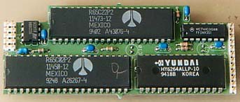
Anyhow, this is all in the back of my mind as I develop POC V2. I'm going to design it so a basic amount of RAM will be on the board (either 512KB or 1 MB), with a socket to plug in more RAM (I may end up using one of Garth's modules as a matter of expediency—he already has a working design). The SCSI controller will be on the same board, eliminating the plug-in HBA and any capacitance it would introduce. The acid test will be to clock the MPU at 20 MHz and see if it can run and remain stable. If it can at that speed, add the memory module and see what happens.
All in good time...
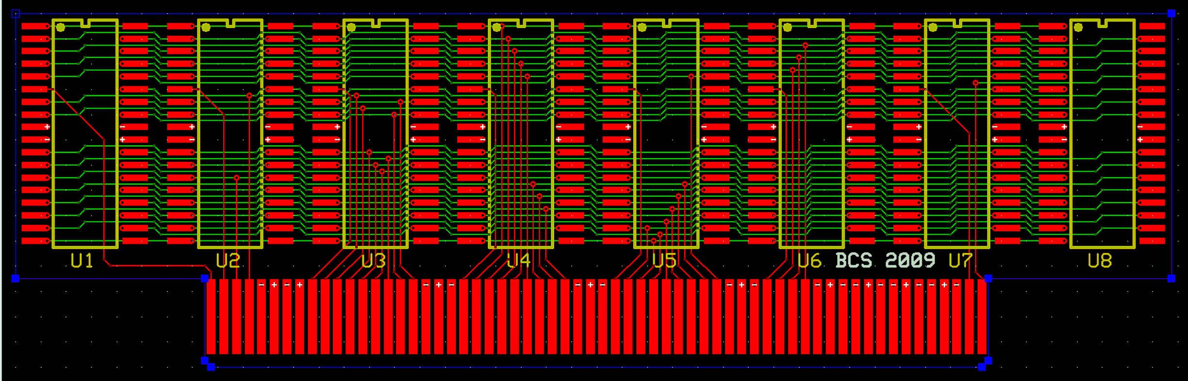
- Segmented memory map, in which the A16-A23 address component brings different RAM into the $0000-$BFFF range, producing an effective range of $xx0000-$xxBFFF, where xx is the segment or bank number ($00-$FF). In this scheme, $C000 and up will always be seen as $00C000-$00FFFF, although different combinations of RAM, ROM and I/O would be possible in that range. Also in this scheme, the bank address emitted on D0-D7 by the '816 during the low cycle of Ø2 would not be used to generate the A16-A23 address component. The CPLD would take care of that, based upon a bit pattern written into a "hardware management unit" (HMU) that would be part of the CPLD logic. In this respect, the CPLD would be mimicking some of the functionality of the MMU in the Commodore 128.
- Linear memory map, in which the A16-A23 address component would be derived from the bank address emitted on D0-D7 by the '816 during Ø2 low. This map would be addressed as $000000-$FFFFFF, assuming a full compliment of 16 MB of RAM has been installed. As you know, the bank address has to be latched on the rise of Ø2, which is tricky to accomplish at higher clock rates when using discrete gates (it can be done with 74ABT logic up to about 14 MHz). Any reasonable CPLD can handle the bank address up to the maximum speed at which the '816 can be run. There are some complications with this model, in that certain conditions (e.g., interrupts) automatically force the program bank back to $00, which is the same bank where all zero page and stack references are directed. Hence something would have to be done to protect bank $00 from improper access. That's outside of the scope of this post.
The '816 is rated as being able to source at least 700 microamps (μA) when an output is high (the Ioh rating) and sink at least 1.6 mA when an output is low (the Iol rating), both ratings when Vcc is 5 volts. WDC doesn't state a maximum output for both states, but it can be inferred from another rating, Idd, which is the no-load current drawn by the '816 for each Mhz. Assuming a maxed out clock rate, Idd would be 40 mA in toto, of which 20 mA would be consumed by the '816's core. Since Iol can be at least 1.6 mA per output and there are 32 outputs, the aggregate minimum current consumption at 20 MHz would be at least 91.2 mA, representing a bit under a 1/2 watt dissipation.
However, in a system of the type I'm contemplating, bus loading would cause Iol and Ioh to substantially exceed the minimums. A particular concern would be the drive strength the '816 could muster when expected to source current. The 700 μA Ioh rating seems weak when one considers the combination of bus loading due to lots of silicon (possibly 32 SRAMS) combined with the inevitable increase in capacitance. I'm thinking that the fanout of the '816 is nowhere near what could be expected from, say, the 65C22, which by design is intended to drive external loads that go beyond what might be expected within the realm of the address and data buses of a microprocessor.
So it seems inevitable that an '816 system that intends to run at high clock rates with a large amount of RAM is going to require line driving of some sort. With a discrete logic circuit, that means using 74ABT541s or similar to drive A0-A15, a 74ABT245 or similar to drive D0-D7 (and isolate them from the '816 during Ø2 low), and a 74ABT573 or similar to drive A16-A23 (and latch them on Ø2 high). A CPLD can produce adequate drive in most cases, assuming it is heat sinked to limit operating temperature. For example, the Atmel 1508AS (a CPLD I'm contemplating) can source about 35 mA per output at Vcc = 5V. Even that may not be enough for a maxed out system running at full throttle, but there's no sure way to determine this without actually building and testing.
My point to all this is I don't think the '816's drive strength can be compared to that of the 65C22 or some of the other I/O silicon. My experience with my POC unit was that the act of plugging the SCSI host adapter (HBA) into the unit forced a reduction in the Ø2 rate. Although the HBA's PCB and the method of interfacing it to the POC inevitably introduced more bus capacitance (effectively, the HBA takes the '816 buses off-board), some of the "blame" lies with the 53C94. I was able to conclude this was the case by simply removing the 'C94 from the socket. When I did so I was able to run the unit at the same Ø2 clock rate as when the HBA wasn't present.
Anyhow, this is all in the back of my mind as I develop POC V2. I'm going to design it so a basic amount of RAM will be on the board (either 512KB or 1 MB), with a socket to plug in more RAM (I may end up using one of Garth's modules as a matter of expediency—he already has a working design). The SCSI controller will be on the same board, eliminating the plug-in HBA and any capacitance it would introduce. The acid test will be to clock the MPU at 20 MHz and see if it can run and remain stable. If it can at that speed, add the memory module and see what happens.
All in good time...