6502.org Forum  Projects  Code  Documents  Tools  Forum
It is currently Mon Apr 29, 2024 6:29 am

All times are UTC


Post new topic Reply to topic  [ 44 posts ]  Go to page 1, 2, 3  Next

would you buy a board with an fpga pre-programmed as a 65Org16?
Poll ended at Sat Dec 10, 2011 7:54 pm
no 50%  50%  [ 4 ]
yes, if it had 40 pin DIL header and space for on board ram 25%  25%  [ 2 ]
yes, if if had 80 I/Os and no space for RAM 0%  0%  [ 0 ]
yes, if it had 80 I/Os and space for RAM 13%  13%  [ 1 ]
any kind at all 0%  0%  [ 0 ]
I'd buy more than one 40 pin board 0%  0%  [ 0 ]
more than one 80 pin with no RAM 0%  0%  [ 0 ]
more than one 80 pin but it must have space for RAM 0%  0%  [ 0 ]
more than one of any kind available 0%  0%  [ 0 ]
I'd buy something for sure but it's not on this list of options 13%  13%  [ 1 ]
Total votes : 8
Author Message
PostPosted: Sat Nov 05, 2011 10:20 am 
Offline
User avatar

Joined: Thu Dec 11, 2008 1:28 pm
Posts: 10793
Location: England
Elsewhere, Garth rubbed a lamp and wished for a 3,3V module with 0.1inch pitch connectors, to provide a 65Org16 CPU in a pre-programmed FPGA:

GARTHWILSON wrote:
... as everything else becomes available in 3.3V, that will be fine.

Quote:
The smallest FPGA that can fit a 6502/65Org16 core are in 100-pin packages, so you would need some sort of 100 to 40-pin adapter for A 6502 core. And a larger adapter for the 16-bit version. At least 32 pins for address, 16 pins for data bus...

If someone could supply them on an optional adapter board with pins to plug into hobby-friendly dual- or triple-row sockets, that'd be great.
Image Image
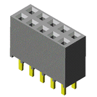
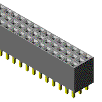
(The picture on the left is about twice actual size and only shows 10 positions, but the socket strips are available in much longer strips that can be cut to the needed size. I know there are WW ones too, but I can't find a picture of one right now.)

I envision the layout being something like:
Code:

                            x x x x x x x x x x x x
 x x x x x x x x x x        x x x x x x x x x x x x
 x x x x x x x x x x        x x                 x x
 x x x x x x x x x x        x x                 x x
 x x x         x x x        x x                 x x
 x x x         x x x   OR   x x                 x x
 x x x         x x x        x x                 x x
 x x x         x x x        x x                 x x
 x x x x x x x x x x        x x                 x x
 x x x x x x x x x x        x x                 x x
 x x x x x x x x x x        x x x x x x x x x x x x
                            x x x x x x x x x x x x

on .100" centers. I don't think anyone expects this to go onto a 40-pin DIP equivalent package.

So I would hope the the FPGA gurus would make these special processors available to all who want to order them, and that the HDL be public domain so if one person doesn't feel like continuing the project, others are not orphaned.


Following on from that, we noted that the HDL is already public domain, and that non-volatile FPGAs do exist, so the board doesn't need too much on it. (Also we had a plea for a 40pin footprint in addition, and a preference for dual row connectors. I think four dual rows might be best, with spacing to allow a subset to serve as a DIL footprint. The dual rows would be half signal, half shield.)

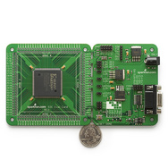
I then realised that such a thing is called an FPGA breakout board. They exist, priced from $50 up. (It still might be worth designing one for our purposes and making a batch, or thinking of it as a business because existing breakout boards just don't have the right feature set.)

Here's an example. It's a two-part board - the left part has not quite enough and the right part adds a bit too much:
Image

See also Pluto boards
Image

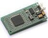
Here are two more with around 50 I/Os, both of which have open source licenses, so could be a basis for a redesign:


Edit: updated title


Last edited by BigEd on Thu Nov 10, 2011 7:54 pm, edited 2 times in total.

Top
 Profile  
Reply with quote  
 Post subject:
PostPosted: Sat Nov 05, 2011 12:58 pm 
Offline
User avatar

Joined: Thu Dec 11, 2008 1:28 pm
Posts: 10793
Location: England
Rough sketch in Eagle of an idea:
Image

The two right hand connectors are spaced to allow use as a 40 pin DIL, or to be stacked onto a 40-pin adaptor. I have no justification for the spacing of the left hand pair.

With 80 I/Os it could serve for a 65Org32. If we didn't want so much shielding then two connectors would be enough.

It lacks
    jtag header for reprogramming
    power converters for the internal voltages
    bypass caps
    any thought about which FPGA pins are pre-assigned

It's quite possible that a two-layer board is impossible (or inadvisable) - the ground geometry on the bottom layers is there for illustration and as an obstruction for the autorouter.

I should submit this to halfbakery.com

Cheers
Ed

ps. Garth's square patterns offer 84 and 80 pins respectively - the problem is leaving room for the 20mm square FPGA and the tracks leading from it. That's feasible (only) if you use surface mount pin headers - didn't think of that. Otherwise, we're left with:
Image


Top
 Profile  
Reply with quote  
 Post subject:
PostPosted: Sat Nov 05, 2011 2:16 pm 
Offline
User avatar

Joined: Fri Aug 30, 2002 1:09 am
Posts: 8428
Location: Southern California
I never do pin headers or sockets in surface-mount since it's too easy to rip the foils off the board with impacts or unplugging (unmating) forces. My PCB layouts for work now are mostly SMT except the connectors that will take some force, and any bigger, heavier parts that could rip the foils away if the product were dropped. Thru-hole pins make it like it's practically rivetted on.

Also, I never autoroute. Autorouters save a lot of time when there's enough room for the design to be autorouted, ie, it's not very dense; but for maximum density and best performance, an autorouter can never compete with a skilled human.

Since EEye and others here are talking about dozens of MHz, then for best performance on this and the board it plugs into, I would definitely want to close up the space between the PQFP and the pin headers up as much as possible. Bypass capacitors, regulators, etc. can probably go on the bottom. (I expect the production volume on this will be so low that it all gets assembled by hand anyway.) When the time comes, I could volunteer the layout work. I have experience in UHF (RF), laying out tiny switching power supplies (where the astronomical di/dt's easily get the inexperienced into trouble), mixed-signal, and can make a digital board well behaved.


Top
 Profile  
Reply with quote  
 Post subject:
PostPosted: Sat Nov 05, 2011 3:06 pm 
Offline
User avatar

Joined: Tue Nov 16, 2010 8:00 am
Posts: 2353
Location: Gouda, The Netherlands
BigEd wrote:
It lacks
    jtag header for reprogramming
    power converters for the internal voltages
    bypass caps
    any thought about which FPGA pins are pre-assigned


I would also suggest adding a RAM chip and some PROM/serial flash for the bitstream and code., as well as the regulators for core/aux voltages.

Putting the RAM on the same board saves a lot of room on the pin headers, and also simplifies high speeds. You can use the pin headers for a slower/narrower bus, or you could put the peripheral logic inside the FPGA, and use the pin headers for I/O.


Top
 Profile  
Reply with quote  
 Post subject:
PostPosted: Sat Nov 05, 2011 3:43 pm 
Offline
User avatar

Joined: Thu Dec 11, 2008 1:28 pm
Posts: 10793
Location: England
Agreed on the regulators, but I think I had them covered (as converters)

I think we can do without the bitstream ROM by using a non-volatile FPGA - it simplifies things and reduces cost, although it rules out spartan6.

(Ultimately, like all such projects, what goes in or not is the call of the person who sits down and starts doing the work. My preference is for minimalism - an FPGA module, not an SBC. But I'm not actually doing the work.)

With memory off-board, we probably have a slower bus (as you say), so a slower FPGA is no great loss. With a lower cost of components more people might be interested.

With memory on-board, we're tending towards a dev board(*) or SBC, can run faster, might go for a spartan 6, and the component cost might double. That will be fine for some, but isn't my preference. That is: I think it's a fine idea, but a different project. (A DIMM socket or two might make sense for that project.)

The spec is done when nothing more can be taken away!

My feeling is that a high performance 65Org16 (or 65Org32) system would be FPGA-based directly, not module based. The module is for getting started, especially for those without FPGA capability. I think it should be cheap(**) - if it's much over $50 there are alternatives already out there. It should be like buying a CPU chip, not like buying a system.

Perhaps one way to tackle this is to address this question: with address and databus connections through these headers, how fast a bus do we think we can run, and how large a 6502-style memory system do we expect to connect to this module?

I suppose there's an obvious companion project which is the motherboard with the socket and the RAM.

Cheers
Ed

(*) and note that EEye is already making progress(***) on a dev board with on-board RAM and spartan6.

(**) but as discussed elsewhere, it's hard to get PCBs cheap unless quantities are quite large. If we can't be cheap, then we might as well be feature-packed. That's an alternative position. It'll take a lot longer - maybe infinitely longer - to come to a conclusion on a rich spec than a minimal one, even if the goal is unpopulated pads for optional components.

(***) EEye is making progress in part because he's going with his own decisions, not trying to please anyone else.


Top
 Profile  
Reply with quote  
 Post subject:
PostPosted: Sat Nov 05, 2011 3:44 pm 
Offline
User avatar

Joined: Thu Dec 11, 2008 1:28 pm
Posts: 10793
Location: England
GARTHWILSON wrote:
I never do pin headers or sockets in surface-mount since it's too easy to rip the foils off the board

Good point.

Quote:
When the time comes, I could volunteer the layout work.

Excellent!


Top
 Profile  
Reply with quote  
 Post subject:
PostPosted: Sat Nov 05, 2011 3:58 pm 
Offline
User avatar

Joined: Tue Nov 16, 2010 8:00 am
Posts: 2353
Location: Gouda, The Netherlands
BigEd wrote:
With memory on-board, we're tending towards a dev board(*) or SBC, can run faster, might go for a spartan 6, and the component cost might double. That will be fine for some, but isn't my preference. That is: I think it's a fine idea, but a different project. (A DIMM socket or two might make sense for that project.)


Well, I was looking at your board, and noticing that the minimum size will be determined the pin headers, anyway, so you won't need to make the board bigger to accommodate a RAM footprint... and to save cost, anyone could decide not to mount the RAM chip, bringing the cost back to the same value as a FPGA-only board.


Top
 Profile  
Reply with quote  
 Post subject:
PostPosted: Sat Nov 05, 2011 4:41 pm 
Offline
User avatar

Joined: Thu Dec 11, 2008 1:28 pm
Posts: 10793
Location: England
I see what you mean - there is a lot of white space. Or blue space, as it happens. It's tricky - I keep wanting to add things too, whether options or unpopulated areas (not just this project, any project) - it's spec creep.

I would say routing a squarely-surrounded breakout board is relatively trivial compared to a system with a functioning bus on board. Do you have Eagle installed? :-)

Cheers
Ed


Top
 Profile  
Reply with quote  
 Post subject:
PostPosted: Sat Nov 05, 2011 9:02 pm 
Offline
User avatar

Joined: Thu Dec 11, 2008 1:28 pm
Posts: 10793
Location: England
So, taking into account Garth's desire for short traces and shielding, and my desire for 80 I/Os, and putting to one side calls for on-board RAM, a 40-pin DIL footprint and for 40-pin or 50-pin cable header compatibility, here's a new sketch:
Image

I don't have components for 3-row connectors so I've improvised. I'm thinking the middle row is a shield row (if that makes any sense at all.)

With as many as 80 I/Os, we can probably afford to include the 4 JTAG signals in that set, so no need for a separate connector for programming.

On the shielding question... 168-pin DIMMs have only approx 35 power/ground signals. Are we overdoing it?

I'm not sure how the bus routing on the motherboard is going to look, with this square footprint. I suppose all modern CPUs have that problem!

Cheers
Ed


Top
 Profile  
Reply with quote  
 Post subject:
PostPosted: Sun Nov 06, 2011 4:52 am 
Offline
User avatar

Joined: Fri Aug 30, 2002 1:09 am
Posts: 8428
Location: Southern California
BigEd wrote:
So, taking into account Garth's desire for short traces and shielding

It's not so much shielding as getting a good transmission line with minimal discontinuities.

Quote:
I don't have components for 3-row connectors so I've improvised.

I have no doubt that your CAD lets you make your own components. I'm always having to make new ones, partly because there are so many parts that the CAD manufacturer could not anticipate.

Quote:
With as many as 80 I/Os, we can probably afford to include the 4 JTAG signals in that set, so no need for a separate connector for programming.

How about if the JTAG header were outboard of the main grid of pins. I doubt that the signals on that are so high-speed, are they?

Quote:
On the shielding question... 168-pin DIMMs have only approx 35 power/ground signals. Are we overdoing it?

The important thing is not the number of them so much as that no signal pin be very far from a ground or virtual-ground pin. The number of ground pins on the pin headers doesn't necessarily have to match the number of ground pins on the IC package.

Quote:
I'm not sure how the bus routing on the motherboard is going to look, with this square footprint. I suppose all modern CPUs have that problem!

I don't finalize the software for microcontrollers I design into products until the board is laid out, because for example I might find that swapping a couple of pins that can do the same functions might make the layout a lot easier or neater or better-behaved or whatever. I suspect you have the same situation with the FPGA; such that the final pinout might be partly determined by the board layout. Anything can be routed with enough layers, but of course we want to keep to the lowest (cheapest) number of layers that will do the job and give adequate transmission-line properties. OTOH, the pinout of the PCB may not be very critical, so maybe that can change more easily than the pin assignments on the FPGA can.


Top
 Profile  
Reply with quote  
 Post subject:
PostPosted: Sun Nov 06, 2011 11:47 am 
Offline

Joined: Mon Mar 02, 2009 7:27 pm
Posts: 3258
Location: NC, USA
GARTHWILSON wrote:
...How about if the JTAG header were outboard of the main grid of pins. I doubt that the signals on that are so high-speed, are they?...

I know we're talking about an AN version of the Spartan 3, but an FPGA PROM programs the FPGA at 6MHz, so I would bet all JTAG signals would be much slower than that.


Top
 Profile  
Reply with quote  
 Post subject:
PostPosted: Sun Nov 06, 2011 12:18 pm 
Offline
User avatar

Joined: Thu Dec 11, 2008 1:28 pm
Posts: 10793
Location: England
I cooked up a plan B, which allows for a number of possibilities:
Image

Ignore the pin assignments - I just wanted to check routability.

In this plan, we have an onboard RAM and a 40-pin DIL header. So now the on-board system might run faster than the off-board system, and we have large (unexpandable) memory rather than huge memory.

Probably the FPGA is now a spartan 6, for extra speed, so we need a PROM for the bitstream. Also we'll need a 6-pin orientable JTAG header. Maybe we need a crystal too.

Plan B1 would expose a footprint very like a 6502, with an 8 bit databus, allowing access to 8 bit peripherals in a 16 bit section of the address space. It could even read out the ROMs of an 8 bit system, although it couldn't directly run from them. (It could run an emulator if that seemed like a good idea.) (Edit: forget this - we don't have 5V compatibility. Unless we add a collection of level shifters. Also note: powering the whole CPU board from a 6502 socket might be a challenge. Back to the half-bakery!)

Plan B2 would trade some address bits for a full 16 bit databus, to allow for 65Org16 peripherals and ROMs (but no chance of an off-board RAM, unless you go for plan B3 which involves the multiplexed bus)

We could have another break out connector for the south edge too.

For this to stabilise as a spec, it has to stop somewhere - that makes me a bit nervous, because I'm not sure where it stops. Unlike plan A, it's not minimal.

Cheers
Ed


Last edited by BigEd on Sun Nov 06, 2011 1:11 pm, edited 1 time in total.

Top
 Profile  
Reply with quote  
 Post subject:
PostPosted: Sun Nov 06, 2011 1:06 pm 
Offline

Joined: Mon Mar 02, 2009 7:27 pm
Posts: 3258
Location: NC, USA
BigEd wrote:
...For this to stabilise as a spec, it has to stop somewhere - that makes me a bit nervous, because I'm not sure where it stops. Unlike plan A, it's not minimal.

Cheers
Ed

Seems we are alike in this regard. I stopped when I ran out of board space!
Might want to keep it simple using Spartan 3AN series, a 55MHz osc., some external speed jumpers with just the CPU core, tristate interface and a DCM .
Just my 2cents...


Top
 Profile  
Reply with quote  
 Post subject:
PostPosted: Sun Nov 06, 2011 4:49 pm 
Offline
User avatar

Joined: Fri Dec 11, 2009 3:50 pm
Posts: 3349
Location: Ontario, Canada
Arlet wrote:
Putting the RAM on the same board saves a lot of room on the pin headers

Including RAM saves the user from quite a lot of work and makes the platform more attractive. But IMO all connections to header pins should still be included.

I realize it's a challenge to route traces if we're to include FPGA, RAM and a large number of header pins. One answer is to move from a 2D to a 3D layout so the RAM chip is directly above or below the FPGA. This is a compelling solution, since all interconnects are uniformly short when both chips are centrally placed! There are two ways to do this:
  • mount the chips on opposite sides of a single board. I created a design using this approach, and of course I was unable to put bypass caps opposite the chips -- they had to mount beside the chips instead. Nevertheless I eventually came up with a PCB I was satisfied with.
  • stack two separate boards one atop the other -- ie, an FPGA board and a RAM board. The header layouts would also stack, meaning that the lower board features a dual-gender connector: female socket on one end, and on the other end a male pin which plugs into the user-built motherboard.
The stacked-board approach is easier to manage, design-wise and for the user. (Some may choose to omit the RAM board, either because they prefer an alternative RAM or in order to connect to some other logic entirely.)

To conclude, my suggestion is to exclude RAM from the FPGA board but to plan and expect that one (or more) stacked boards will share the header pinout. It would be terrific if the same team could produce FPGA and RAM boards. The labor would be comparable to a single board with both chips.

-- Jeff


Top
 Profile  
Reply with quote  
 Post subject:
PostPosted: Sun Nov 06, 2011 8:29 pm 
Offline
User avatar

Joined: Fri Aug 30, 2002 1:09 am
Posts: 8428
Location: Southern California
If you want the RAM to go with it, my suggestion, for both cost and performance, would be to put the RAM IC on the opposite side of the same board. Besides having one less board to pay for tool-up on, the performace that way will be better than going through another set of headers and pins, even though the bypass capacitors can't be directly under the pins of both ICs. (They might be able to be under the pins of the FPGA if it is larger than the RAM IC though.)


Top
 Profile  
Reply with quote  
Display posts from previous:  Sort by  
Post new topic Reply to topic  [ 44 posts ]  Go to page 1, 2, 3  Next

All times are UTC


Who is online

Users browsing this forum: No registered users and 9 guests


You cannot post new topics in this forum
You cannot reply to topics in this forum
You cannot edit your posts in this forum
You cannot delete your posts in this forum
You cannot post attachments in this forum

Search for:
Jump to: