Page 1 of 2
65org16 Interest
Posted: Thu Nov 03, 2011 9:00 pm
by kc5tja
I just wanted to express how awesome I think it is that folks here are experimenting with the 65org16 architecture. Since both the J1 processor and the 65org16 expose a 16-bit byte to the world, sharing peripherals between them should be pretty simple.
Posted: Thu Nov 03, 2011 10:04 pm
by BigEd
That's a good thought!
I'm already keeping an eye on
your source, as you know.
I see you have, or are working on, a (monochrome) graphics adapter and a ps/2 interface.
Cheers
Ed
Posted: Thu Nov 03, 2011 10:29 pm
by kc5tja
The PS/2 interface should be complete.
The MGIA aspect of the UXA should similarly be complete, but, it doesn't expose a bus interface to the host processor yet. That is, it's fully capable of rendering an image, but you have to program the FPGA's initial SRAM image with the bitmap first. Put another way, the bus interface to the video memory will be added once I have a working processor module to poke bytes in with.
If anyone expresses interest, I can add the bus interface sometime next week (someone remind me, please). I won't be able to get to it at least until this coming Monday.
Posted: Fri Nov 04, 2011 12:16 am
by Dajgoro
I've been seeing a lot about the 65org16 lately. But i am wondering if it is possible to have one at all? Fpga parts are out of reach for a lot of people(including me), so i am wondering if it is going to get a bit more accessible for other people.
Posted: Fri Nov 04, 2011 12:44 am
by ElEctric_EyE
When I first started working with cores, I thought about just putting a core all by its lonesome inside an FPGA, with some tri-state interfacing...
There's a few problems, not insurmountable, but read on:
First and foremost, voltage! You guys want 5V levels. That will only be possible if you can stuff it inside an older style CPLD. Even if it is possible, it will most likely be a larger 208-pin package. 3.3V levels would be much more likely, and much faster.
The smallest FPGA that can fit a 6502/65Org16 core are in 100-pin packages, so you would need some sort of 100 to 40-pin adapter for A 6502 core. And a larger adapter for the 16-bit version. At least 32 pins for address, 16 pins for data bus...
Then, think of address decoding a 32-bit address bus with external TTL. Instead of that, use the few leftover pins on the 100-pin FPGA, and internalize the adress decoding, and you might be in business for something, but then it would have to be standardized... When you start to get into it yourself at this point, you see why there is no market for this type of thing. Because once you get into it yourself, everything previously mentioned becomes a non-issue!
Posted: Fri Nov 04, 2011 2:18 am
by GARTHWILSON
Ideally, yes, but as everything else becomes available in 3.3V, that will be fine. Right now I still tend to lean to 5V just a little because of other things I want to interface to, but in a few years it might not be that way.
The smallest FPGA that can fit a 6502/65Org16 core are in 100-pin packages, so you would need some sort of 100 to 40-pin adapter for A 6502 core. And a larger adapter for the 16-bit version. At least 32 pins for address, 16 pins for data bus...
If someone could supply them on an optional adapter board with pins to plug into hobby-friendly dual- or triple-row sockets, that'd be great.
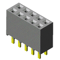
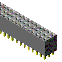
(The picture on the left is about twice actual size and only shows 10 positions, but the socket strips are available in much longer strips that can be cut to the needed size. I know there are WW ones too, but I can't find a picture of one right now.)
I envision the layout being something like:
Code: Select all
                            x x x x x x x x x x x x
 x x x x x x x x x x        x x x x x x x x x x x x
 x x x x x x x x x x        x x                 x x
 x x x x x x x x x x        x x                 x x
 x x x         x x x        x x                 x x
 x x x         x x x   OR   x x                 x x
 x x x         x x x        x x                 x x
 x x x         x x x        x x                 x x
 x x x x x x x x x x        x x                 x x
 x x x x x x x x x x        x x                 x x
 x x x x x x x x x x        x x x x x x x x x x x x
                            x x x x x x x x x x x x
on .100" centers. I don't think anyone expects this to go onto a 40-pin DIP equivalent package.
Then, think of address decoding a 32-bit address bus with external TTL.
Although the double-wide address bus would be 32-bit, I don't expect anyone will really need all 32 bits brought out. Also, the address decoding need not be complex. It can be nearly as simple as what I have on the workbench computer (diagram
here) where RAM, ROM, and up to 10 I/O ICs can all be handled through three of the four sections of a single quad NAND IC; and that logic could be put in the FPGA also.
So I would hope the the FPGA gurus would make these special processors available to all who want to order them, and that the HDL be public domain so if one person doesn't feel like continuing the project, others are not orphaned.
Posted: Fri Nov 04, 2011 5:55 am
by BigEd
I've been seeing a lot about the 65org16 lately. But i am wondering if it is possible to have one at all? Fpga parts are out of reach for a lot of people(including me), so i am wondering if it is going to get a bit more accessible for other people.
Do you mean out of reach due to cost, or because of the learning curve, or the surface mount soldering, or the 3.3v interfacing? I admit there are several possible reasons, and maybe all of them apply.
A 40/50-pin OHO module board starts at
50 EURO plus postage - that solves the surface mount, fine pitch and voltage problems, if the cost is OK. It leaves you with the learning curve, a couple of connectors to solder, and gives you a 40-pin limitation. That allows you a multiplexed 16-bit data and 24-bit address bus in a mostly 6502-style pinout. You could squeeze a few more address bits out too. You'd need external address latches, like for a 65816.
For a standard module like that, we could come up with a bitstream which anyone could use to work like a standard pinout - there need not be a learning curve, you need not engage with verilog.
Low-end FPGA chips themselves seem to start around £10, but postage is going to add to that - that leaves you with board design, soldering and the voltage problem. Plus the learning curve. It's quite possible, my point here is that cost needn't be prohibitive for the FPGA - the cost of the boards will be the biggest part of it.
(We only need 50% of the smallest xilinx FPGA - the
XC3S50A)
For the voltage problem, if it is a problem,
SN74CB3T16211 24-bit level converter is £4 - that's if you want to do a mixed-voltage design.
Posted: Fri Nov 04, 2011 6:12 am
by BigEd
So I would hope the the FPGA gurus would make these special processors available to all who want to order them, and that the HDL be public domain so if one person doesn't feel like continuing the project, others are not orphaned.
! (Thanks to Arlet for clarifying the license.)
The processors could be - or are - available in the sense that we could help with standard bitstreams for any standard board designs - EEye's dev board would be one, any commercial FPGA module or dev board would be another. With FPGA, what matters is choosing a pinout and defining the timing boundary. Any board design will need to include the EEPROM(*) for the bitstream too. We're not in a position to make a chip for you, but it's the next best thing - the end user will need to design in an FPGA, or take the cost of using an FPGA module.
Edit: ah, I see you're asking for someone to design a 65Org16 module and sell it. That's an idea... but I don't think it will be me, sorry. Personally I favour the OHO module - does the 50-pin version suit? Ruud has
taken that route. Instead of one of us doing the design and manufacture and buying parts ahead of time, some small company does it. If you can do it cheaper or better though, go for it.
Edit to add:
(*) or use a non-volatile FPGA such as xilinx spartan-3AN series (
pdf)... and as these exist, one could actually program one as a 65Org16 and resell it. Just need to decide on an acceptable pinout.
Posted: Fri Nov 04, 2011 12:53 pm
by Nightmaretony
would lean towards the dual row as 50 pin headers for ribbon cables are pretty cheap to get and you can get pins for that setups fairly easily. Think of the security board on the Capcon CPS 2 arcade game system
http://www.system16.com/hardware.php?id=793
(k, the sub board ones don't show but the side ones do which are also 50 pin dual row ones. Most famous game on this motherboard set: Street Fighter ][....
Posted: Fri Nov 04, 2011 4:52 pm
by Dr Jefyll
I don't expect anyone will really need all 32 bits brought out.
This triggered a train of thought for me, and I ended up in an unexpected place. What would be the Costs versus Benefits of
other widths -- a 65Org
12, for instance?
Yes I know 12 isn't a power of two, and that may take some getting over. Powers of two have a strong intellectual appeal! But in concrete terms the power-of-two benefits don't seem compelling. It's true that 65Org
16 would have an advantage when it comes to rewriting existing 8-bit code. Eg: a double-precision addition translates directly to single precision. (What are some other examples? I'd be happy to hear them, but right now I want to look at the flip side.)
65Org
10 would be a natural for, say, a product that had to store and sort 10-bit samples from an ADC. Or, looking at the address side of things, a 65Org
12 might do nicely for applications requiring a 24-bit (16 MB) address space.
At the hardware level, 65Org
16 is expensive in terms of pins (as mentioned in the discussion about prototype boards). 65Org
12 alleviates the pinout problem, although it raises the question of how to implement off-chip memory. Would you use byte-wide devices to create a 16-bit memory, and then waste 4 bits? Or
are those 4 bits an opportunity to implement a virtual-memory tag or some other imaginative scheme?
Finally, 65Org
9 hits a sweet spot in several ways. In addition to quadrupling the 6502 address space, it would create 256 new opcodes to exploit. So, the implications of going from 8 bits to 9 are far from trivial! And 9-bit word widths are supported internally by certain Programmable Logic devices and on the external level by memory devices (typically intended for applications using parity error detection). 9 bits could turn out to be an amazingly good fit for some jobs!
Cheers, and apologies to Arlet and Ed if I'm rocking the boat, Verilog-wise, with these suggestions...

-- Jeff
Posted: Fri Nov 04, 2011 5:48 pm
by BigEd
Curious and interesting! The availability of 9-bit wide memories helps the case a lot. I don't think there are any other barriers - I'm speaking for others but I would think the assemblers should be OK. The code may not be as freely parameterisable as the verilog is, but is presumably adjustable with some effort - and as they are both open source, the inventor can bear the burden!
Using 16bit wide memory on a 12bit wide system and tagging the accesses could be quite something too. Are we headed for the
Burroughs B5000 rebuild?
(I may be a bit of a broken record over this [a phrase from the vinyl generation] but we don't need to expose all 32 bits of an address bus for 65Org16, and we can multiplex with the databus if we have to - the 65816 shows that. So, squinting at the 6502 pinout, I can lose or repurpose 6 pins before I start, which gives me pinouts ranging from 26 pins for a 16bit address bus to 40 pins for a 30bit address bus. The 6 pins would be 3 no-connect, phi1 out, sync and so. Or, we use a 50-pin module and drop the multiplexing. Or, we interface to a memory which multiplexes high and low addresses internally.)
Posted: Fri Nov 04, 2011 6:10 pm
by ElEctric_EyE
Won't one run into problems with indirect indexed mode, when the data bus/address bus is not a multiple of 8? i.e. 8, 16, 32
Posted: Fri Nov 04, 2011 6:13 pm
by BigEd
I don't think so - it's just like the move to 16-bit bytes really, you just have to make the mental adjustment that a 'page' is a different size to what you thought it was. There are still two halves to an address. (Anywhere you count up to 8 will need adjusting, and rotates might need consideration.)
Posted: Fri Nov 04, 2011 6:55 pm
by GARTHWILSON
Yes I know 12 isn't a power of two, and that may take some getting over. Powers of two have a strong intellectual appeal! But in concrete terms the power-of-two benefits don't seem compelling. It's true that 65Org16 would have an advantage when it comes to rewriting existing 8-bit code. Eg: a double-precision addition translates directly to single precision. (What are some other examples? I'd be happy to hear them, but right now I want to look at the flip side.)
Going in multiples of 8 makes better use of available memory types. Is 9-bit-wide memory available in the easiest-to-use types (SRAM and ROMs)? I doubt it. The HP-71 hand-held computer which was introduced in 1983 was an incredible example of outstanding system engineering from the standpoint of having plug-and-play
ten years before they were even
talking about in on PCs, interfacing to a virtually unlimited number of peripherals at once, the user being able to extend the OS, having local environments, user control of interrupts and their servicing, and a ton of other marvels, and being nearly bug-free; but it has a 4-bit data bus, a 20-bit address bus, and 64-bit processor registers. (The 64-bit registers were for efficient implementation of the IEEE floating-point standard before it was even a standard but its passage was anticipated.) The strange implementation actually had some good reasons, based on the application and the technology available at the time. ANS Forth requires that the number of bits in a cell be a power of two, 16-bit minimum, but it's not like it were the law. There are other things about ANS Forth I won't ever be going along with. Forth on the HP-71 had 20-bit cells, which along with 4 bits per address (and two addresses per text character), was kind of strange, but did not present any problems in my experience. But in situations where 16-bit was a little limiting for the standard numbers you wanted to use, 20-bit avoided much of the potential need for doubles which now would be 40-bit instead of 32.
(I may be a bit of a broken record over this [a phrase from the vinyl generation] but we don't need to expose all 32 bits of an address bus for 65Org16, and we can multiplex with the databus if we have to - the 65816 shows that. So, squinting at the 6502 pinout, I can lose or repurpose 6 pins before I start, which gives me pinouts ranging from 26 pins for a 16bit address bus to 40 pins for a 30bit address bus. The 6 pins would be 3 no-connect, phi1 out, sync and so. Or, we use a 50-pin module and drop the multiplexing. Or, we interface to a memory which multiplexes high and low addresses internally.)
Without knowing for sure, I suspect the 816's reason for the address bus multiplexing had to do with the cost of lead frames and IC sockets of more than 40 pins (before PLCCs came along), and the longer connections in those lead frames as they looked forward to higher speeds, also being able to make a board that with a few jumpers could use either the 6502 or the '816. Samuel wrote here one time that the cost of testing goes up quickly as you add pins. Maybe DC@wdc (new member here) can tell us, if indeed he's reading this. I would certainly prefer not to have to add the external latch to go above 64K of address space. That scheme seems to reduce the maximum speed of the '816 a little bit compared to the 6502 also.
What I meant by not bringing all the address lines out is that probably no one would be using more than say 16Mx16 of memory map in a system like this. For that, 24 bits of address bus would be enough, with no multiplexing.
If this FPGA is really going to allow bus speeds of 32 or 50 or more MHz though, you're going to have to leave the module a lot of pins for ground and Vcc. Just one or two won't do, especially on something big enough to get the pins on .100" centers. On my
4Mx8 5V SRAM module (data sheet
here) which I have available with 10ns SRAM chips, no signal pin is more than .2" away from a ground or bypassed Vcc pin.
http://WilsonMinesCo.com/
Posted: Fri Nov 04, 2011 7:25 pm
by BigEd
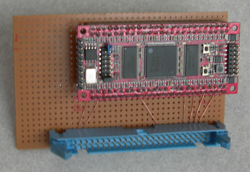
yes - it so happens that the 50-pin OHO connects with two 50-pin dual-row connectors, which each carry just 25 signals (or 24)
These
two pictures by Ruud for his
RB6502 project give some idea.
Fair point about bus multiplexing - it's probably only worthwhile for moderate speeds and where pin count is a major limitation.
On the module front, do we need any more than a non-volatile FPGA with suitable bypass caps, voltage regulators, and a jtag header, on a board with a couple of 50-pin connectors? (The simpler the spec, the more likely it is to happen.)
That module commits the end user to nothing more specific than some 3.3v 50-pin application of an FPGA - it doesn't even have to be a CPU, although it could be shipped as one.
Could be more than 2x50 connectors I suppose. 4x40 in a square might be something like your picture, and would give up to 80 I/Os.
Fancy going into business with that?
Cheers
Ed