Page 1 of 4
4MB SRAM Module
Posted: Fri Aug 19, 2011 11:45 pm
by 8BIT
Hi All,
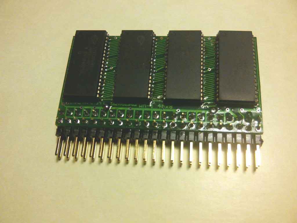
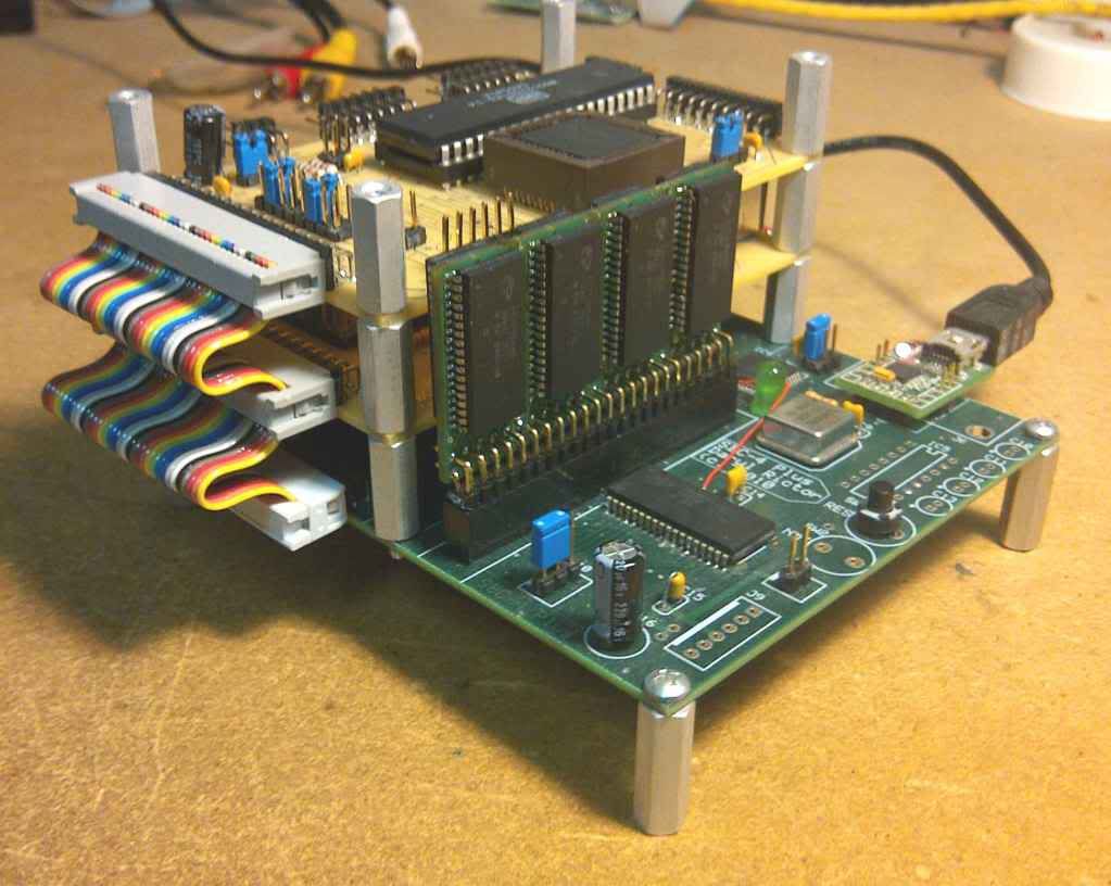
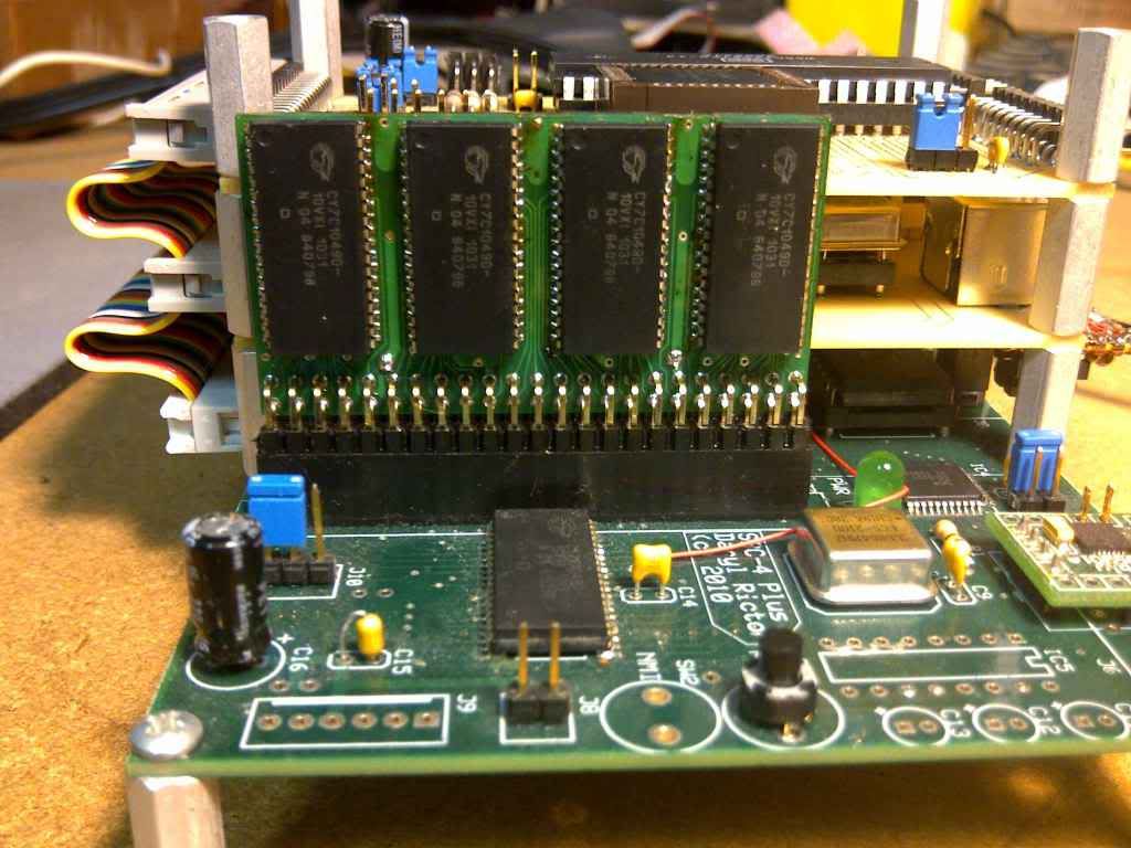
Garth Wilson has designed and created a 4MB SRAM module that can be used for our projects. I have tested these on my SBC-4P and they work great. They are very compact and did not seem to add a significant amount of bus loading to my system. I was able to run my SBC-4P with three expansion cards and the memory module at 12MHz without any issues.
These will be perfect for applications that require a large amount of SRAM without taking up acres of board space.
The board has SRAM chips on both sides - 8 total.
Here are a few pictures of Garth's module:
Daryl
Posted: Fri Aug 19, 2011 11:59 pm
by Dajgoro
And just yesterday i was looking for something like this, i thought about building some kind of digital signal analyser module, which would record digital signals into ram, and then use the 6502 to preview the recorded data, i already made something similar with a pic16f877 and a 8x8 led display, but it only has 256 bytes for recording...
Re: 4MB SRAM Module
Posted: Sat Aug 20, 2011 4:36 am
by BigDumbDinosaur
Garth Wilson has designed and created a 4MB SRAM module that can be used for our projects.
Oooh, looks like the SIP RAM modules we used to put into BASIC Four minicomputers back in the 1980s.

Only difference, they didn't have 4 MB per module. It was more like 64K per module and each one cost a bunch.
Posted: Sat Aug 20, 2011 5:49 am
by GARTHWILSON
Oooh, looks like the SIP RAM modules we used to put into BASIC Four minicomputers back in the 1980s. :lol: Only difference, they didn't have 4 MB per module. It was more like 64K per module and each one cost a bunch.
Posted: Sat Aug 20, 2011 7:43 am
by BigEd
Very nice indeed!
Memories...
Posted: Sun Aug 21, 2011 5:23 am
by BigDumbDinosaur
I don't recall anymore the precise layout but it was DRAM. There was a TI DRAM controller on the motherboard. Almost everything was in discrete logic, so the motherboard had more 74LS silicon on it than you could shake a stick at. These minis mostly had full height ST-506 hard disks, with the controller on the motherboard. Eventually, Basic Four switch to SASI and then SCSI disks.
The SIP memory module was a bit of a pain because it was quite easy to bend a pin. If one wasn't very careful in straightening the bent pin it would break off, ruining a module that, if memory correctly serves me, cost about 200 bucks. Later machines switched to SIMM packages, which, of course, were much more forgiving.
Posted: Sat Sep 17, 2011 5:50 am
by GordonZaft
So where can I get one, and where does one get 512Kx8 SRAMs?
Posted: Sat Sep 17, 2011 5:52 am
by GARTHWILSON
So where can I get one, and where does one get 512Kx8 SRAMs?
Contact me offline and I can get you one or more modules. I will assemble them here, so you don't have to buy the SRAM ICs. There's one part of the assembly that is particularly tricky (involving the embedded bypass capacitors), so I'm not fond of the idea of selling bare boards or kits.
Posted: Sat Sep 17, 2011 6:18 am
by GARTHWILSON
Below is some of the info on the module. Pictures are already above.
- 4Mx8 5V SRAM module, 2.300" long x 1.234" wide, not including connector
- has eight 10ns Cypress CY7C1049D-10VXI 512Kx8 5V SRAMs, four on each side. See Cypress data sheet at http://www.cypress.com/file/221601/download (Keep the total capacitive bus loading in mind when estimating actual speed performance predictions.) Note, 9/28/18: Cypress occasionally makes teensy changes in the silicon process or bond wires or something else that has zero effect on us hobbyists, and then change the part number, and then people look it up and get scared thinking it's been discontinued. No, I'm sure they'll have it available for many years to come, maybe decades. I have a legitimate business and a resale number, and I buy 100 at a time from commercial Cypress distributors in the U.S. who don't sell to mere hobbyists, at half of Digi-Key's price. Edit, in 2020: When I went to buy more SRAMs, Cypress's prices had gone way up, so I went to the ISSI equivalent, whose data sheet is at http://www.issi.com/WW/pdf/61-64C5128AL.pdf .
- six embedded (for minimum inductance) .1uF bypass capacitors
- four ground pins and two Vcc pins, distributed so no signal pin is more than .2" away from a ground or bypassed Vcc pin
- eight separate CE\ pins, so you can get faster selects by handling the computer's entire address-decoding scheme with a CPLD if desired than you would get from adding a 74xx138 to this plus the computer's other address-decoding logic
- two WE\ pins, one for each set of four ICs, so your circuit can write-protect half at a time if desired
- two OE\ pins, one for each set of four ICs
- two-layer board's high-speed performance is maximized by unorthodox layout and bypass chip capacitors under the ICs actually embedded in the board for minimum inductance
- 46-pin dual-row header of .025" square posts on .100" centers, to plug into readily available, inexpensive thru-hole sockets on your prototyping boards (I can supply the sockets too)
- symmetrical pin-out lets you plug it in backwards and it will still work! (This is possible with SRAM because as long as data lines go do data pins, it doesn't matter if they get mixed up; the same goes for address lines, and the same goes for CE\ lines. I have also done this with EPROM to make the board easier to route, and then used a programming adapter.)
- available with straight or 90° pins
- partial assemblies in increments of half megabyte available for lower prices, using the same board. Even if you only get one or two SRAMs on the board, one advantage to you may be the easier assembly of your computer because of the pin header (ie, not having to solder with SMT-only devices), less time required to build your computer, be able to build it on perfboard (although for such fast parts I still recommend using at least a ground plane on one side like Twin Industries' 8100-series protoboards ( http://twinind.com/subcategory/plated-t ... ngle-power ) if not also a Vcc plane on the other side like Twin Industries' 8200-series protoboards ( http://twinind.com/subcategory/plated-t ... dual-power ) and keep parts as close together as possible and wire-wrap wires as short and straight as possible without straining them.)
Edit, 2/25/12: Data sheet now available at http://wilsonminesco.com/WM-1_4Mx8SRAMmodule1-2-17.pdf . Later updates for Cypress' updated data sheet on the ICs. Edit again: Updated http://wilsonminesco.com/WM-1_4Mx8SRAMmodule4-23-20.pdf
Posted: Sat Sep 17, 2011 11:59 am
by ElEctric_EyE
...[*]symmetrical pin-out lets you plug it in backwards and it will still work! (This is possible with SRAM because as long as data lines go do data pins, it doesn't matter if they get mixed up; the same goes for address lines, and the same goes for CE\ lines. I have also done this with EPROM to make the board easier to route, and then used a programming adapter.)
I like that!
80mA is a pretty low operating current for a larger SRAM.
Posted: Sat Sep 17, 2011 4:51 pm
by Dr Jefyll
I have also [mixed up the lines] with EPROM to make the board easier to route, and then used a programming adapter.
Footnote: there are advantages to simply making a programming adapter, but we should remember it's not the only alternative. It's possible instead to write a routine to pre-scramble the binary image file before you burn it into the EPROM. It's done in such a way that the scramble of the binary array beforehand and the scramble of the pin-swaps in the target system are complementary -- resulting in no scramble at all. You can even arrange to use
two software pre-scrambles in sequence, which will let you deal with Address pins that are mixed up (among themselves)
and Data pins that are mixed up likewise. Better have a fresh pot of coffee on hand when you write the routines, though; the code's not horribly complicated, but you do need to be meticulous!
-- Jeff
Posted: Sat Sep 17, 2011 6:17 pm
by GARTHWILSON
80mA is a pretty low operating current for a larger SRAM.
I didn't mention the current myself, but the data sheet says 90mA is the maximum current and maximum speed and 100% duty cycle (a condition we will not be hitting on 6502's and 816's), and then it will only be for the one SRAM chip that's active at a time. The other seven will be sleeping.
Footnote: there are some advantages to simply making a programming adaptor, but as you probably know it's not the only alternative. Instead you can create software to pre-scramble the binary image file before you burn the EPROM.
I would have done that if I had made my own EPROM programmer controlled by my workbench computer; but since this was on the PC and I don't program PCs, the socket adapter was a quicker solution. Then of course you can read it back in without the adapter and store it in another file so future EPROMs can be programmed without the adapter.
Posted: Sun Sep 18, 2011 12:40 am
by teamtempest
It's possible instead to write a routine to pre-scramble the binary image file before you burn it into the EPROM.
Do you mean something like this?
http://srecord.sourceforge.net/
I haven't used this myself, but my impression on looking at the various "input filters" was that they're meant to accomodate strange EPROM addressing schemes.
Posted: Sun Sep 18, 2011 3:00 am
by Dr Jefyll
It's possible instead to write a routine to pre-scramble the binary image file before you burn it into the EPROM.
Do you mean something like this?
http://srecord.sourceforge.net/
No. (Some interesting stuff there, though.) Imagine you're designing a circuit board that includes an EPROM and a CPU. Normally you'd connect d0 of the CPU data bus to d0 of the EPROM, and CPU d1 to EPROM d1 and so on. But imagine that there are physical layout issues, and,
to accommodate the layout you want, you connect...
- CPU d0 to EPROM d4
CPU d1 to EPROM d5
CPU d2 to EPROM d6
CPU d3 to EPROM d7
CPU d4 to EPROM d0
CPU d5 to EPROM d1
CPU d6 to EPROM d2
CPU d7 to EPROM d3
In other words the board wiring causes the CPU to "see" the EPROM data as having its hi and lo nybbles swapped. (It's an unlikely example, but easy to discuss.)
To compensate, the "pre-scramble" is performed on the binary image of the EPROM data before it's blasted into the EPROM. Say the first byte is 34h; it will be replaced with 43h. Say the 2nd byte is 69h; that'll get switched to 96h. And so on -- every byte in the binary image has its nybbles swapped. Then the EPROM is burned and removed from the programming socket. When it's plugged into the socket on your board, the CPU will read the EPROM data as being normal -- ie; the hi and lo nybbles appear back where they belong.
Depending on the layout, you may choose to scramble the address lines instead of the data lines -- or scramble both (but not with each other, of course). The wiring you adopt will determine the pre-scramble you require.
Pre-scrambling yielded an immense advantage when I mod'ed
a dozen bizarre, embedded, discrete-TTL processor boards years ago. My goal was to hack the code, which -- rather inconveniently -- was stored in 82S115 TTL PROMs. I opted to replace the TTL PROMs with EPROMs, but the pinouts matched very poorly! Without the scramble trick I would have had to wire-mod almost all of the 24 pins on every socket. Instead there were only a few.
-- Jeff
Posted: Sun Sep 18, 2011 3:40 am
by Dr Jefyll
- two-layer board's high-speed performance is maximized by unorthodox layout and bypass chip capacitors under the ICs actually embedded in the board for minimum inductance
Capacitors embedded in the board? Cool! That would be underneath an IC, then, right? I've wondered about trying something like that. Care to share the details, and a photo maybe? Sounds like you'd have to use a chisel or router to create a cavity in the PCB material...
-- Jeff
ps- lovely job on the RAM module!