Page 1 of 1
6522 VIA for SPI (SD cards...)
Posted: Wed Oct 27, 2010 1:55 pm
by jesari
While designing a SD card interface to my own 6502 SBC i read this on André Fachat's 8-bit pages:
SD cards require SPI mode 0, while the VIA's shift register is SPI mode 3. "You could reverse clock, but you cannot make the VIA shift out earlier. So there is no way to use the VIA SR".
Well, you can't make the SR shift out earlier, but you can delay the clock. I did this using a 1us delay line made of 4 RC networks and HC04 inverters and I got a 500 kbit/sec SD interface directly from CB1,CB2 pins. For input I used a 74HC164 shift register clocked by the same delayed and inverted clock. This register is connected to the full port B of the VIA.
And for level conversion I'm using simple resistive voltage dividers for SCK, MOSI and /SS, while MISO is connected directly to the HC164.
All the timings are for 1MHz phi2 clock.
I just finished a working prototype. It can fill the whole 56kB of RAM from a SD card in less than 2 seconds (about 24 cycles/byte) I don't think the same speed is possible using bitbanging.
The same interface can be also used with an ENC28J60 Ethernet module, but it is not yet tested.
Posted: Wed Oct 27, 2010 2:52 pm
by Nightmaretony
VERY sweet. Hope you can post schemartics and code eventually, make more of a canonical base for interfacing projects...
Posted: Thu Oct 28, 2010 7:22 am
by jesari
The schematic is availabe from the following URL:
http://www.ele.uva.es/~jesus/6502/perif_schem.pdf
Posted: Thu Oct 28, 2010 2:27 pm
by Nightmaretony
A most clever and working design. For giggles, I will redraw as specific to port, on general principles. I had seen SD interface for the AVR as is for everything else, but super glad to see a working 65XX series interface

Posted: Thu Oct 28, 2010 11:05 pm
by kc5tja
That is really slick. I like it!
Though, why do you have resistors on only three of the PB pins? It seems as though you set those pins to output under certain conditions. Are they used for other purposes besides reading the peripheral feedback?
Posted: Fri Oct 29, 2010 2:07 am
by ElEctric_EyE
jesari, how long have you been working on your SD card interface?
Seems like you are you using the 6522 just for 8 bit output port?
I also would like to use "solid state" memory... Your SD card interface seems much easier, than a USB interface IC I've been thinking about.
Posted: Fri Oct 29, 2010 7:35 am
by jesari
That is really slick. I like it!
Though, why do you have resistors on only three of the PB pins? It seems as though you set those pins to output under certain conditions. Are they used for other purposes besides reading the peripheral feedback?
After reset the current ROM code sets those bits as outputs. This has to be changed on new revisions, but, meanwhile, the resistors help to relax data contention.
Posted: Fri Oct 29, 2010 8:10 am
by jesari
jesari, how long have you been working on your SD card interface?
Seems like you are you using the 6522 just for 8 bit output port?
I also would like to use "solid state" memory... Your SD card interface seems much easier, than a USB interface IC I've been thinking about.
The building took around une week of my spare time, but I was thinking about it long before, since I built the CPU board (Feb. 2010)
The PORTB of the VIA is used only for input, while PORTA is used also for other interfaces: bitbanging UART, I2C and speaker. PA0 is the ROM enable signal in the CPU board, so it can't be used for I/O. I'm keeping ORA always as $00 and changing DDRA instead.
The SD interfacing is much simpler than USB, as you can see. The software can be also much simpler than that for USB. I'm right now dealing with the FAT16 filesystem...
Posted: Fri Oct 29, 2010 11:29 am
by jesari
Here are some details related to the code involved. First a timming diagram:
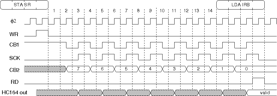
It is clear that a minimum 14 cycles are needed between SR write and IRB read.
And the code involved:
Code: Select all
; Single transfer
; 14 cycles between WR and RD
spibyte:
	        sta	SR	   ; 4 cycles
	        jsr	delrts  ; 12 cycles
	        nop		     ; 2 cycles
	        lda	IRB	  ; 4 cycles
delrts:    rts
In order to achieve a higher speed with the SD card, I'm using the following routines for block transfers:
Code: Select all
; Block transfer (up to 256 bytes), write
; ptr1 ->  data source
; Y: # of bytes (minimum:1, 0=256)
; 19 us/byte (421 Kbit/s)
;------ Not yet tested ------
spiwr:
	sty	tmp1
	ldy	#0
spiwr1:
	lda	(ptr1),y	; 5 cycles
	sta	SR		; 4 cycles
	nop			; 2 cycles
	iny			; 2 cycles
	cpy	tmp1		; 3 cycles
	bne	spiwr1		; 3 cycles
	rts

; Block transfer (up to 256 bytes), read
; ptr1 <- data destination
; Y: # of bytes (minimum: 2 bytes, 0=256)
; 22 us/byte (363 Kbit/s)

spird:
	ldx	#$ff
	stx	SR		; 4 cycles (dummy write)

	dey			; 2 cycles
	sty	tmp1		; 3 cycles
	ldy	#0		; 2 cycles
	nop			; 2 cycles
	nop			; 2 cycles
	beq	spird1		; 3 cycles

spird1:
	lda	IRB		; 4 cycles
	stx	SR		; 4 cycles (dummy write)
	sta	(ptr1),y	; 6 cycles
	iny			; 2 cycles
	cpy	tmp1		; 3 cycles
	bne	spird1		; 3 cycles / 2 cycles if no taken

spird2:
   nop			; 2 cycles
	lda	IRB		; 4 cycles
	sta	(ptr1),y
	iny
	rts
The SD sector is 512 bytes long, and, therefore, I'am calling spird twice
Posted: Sun Oct 31, 2010 9:50 pm
by APL
The same interface can be also used with an ENC28J60 Ethernet module, but it is not yet tested.
What a sweet little interface. Presumably brings the potential to use devices like the 'Connect Wi Fi' wifi cards to the table.
http://uk.eye.fi/
PS. I only own one which my camera couldn't cope with, so it's just sitting there.
Re: 6522 VIA for SPI (SD cards...)
Posted: Sun Jan 13, 2013 3:19 pm
by fachat
Hi there,
I have updated my SPI page, where I now have extended my SPI interface to use SPI mode 0 as well.
I'm not using a delay, but an inverter (xor) in the data line to manually set the first data bit before shifting out the
rest of the data.
Runs at any speed up to phi2/2 (shifting out at phi2).
http://www.6502.org/users/andre/csa/spi/index.html
Andre
Re: 6522 VIA for SPI (SD cards...)
Posted: Fri Jan 02, 2015 8:11 pm
by BigEd
[As jesari's schematic is on a web server not presently responding, here's an archive link:
http://web.archive.org/web/201206281353 ... _schem.pdf
It's a subpage of "Bender's brain. A 6502 prototype" at
http://web.archive.org/web/201306201645 ... proto.html
]