Getting started with Xilinx CPLD's & FPGA's
Posted: Mon Oct 18, 2010 12:41 pm
All info in this thread applies to the first steps needed to interface Xilinx CPLD's and/or FPGA's to an "x86 PC" using the JTAG interface along with the Xilinx ISE software, in an effort to successfully program these CPLD's/FPGA's. Your PC will need 1 port for the JTAG interface, typically either a parallel or USB interface.
Previous knowledge of basic TTL/CMOS logic design is assumed.
If you are ready to get your "feet wet" using programmable logic arrays and are starting a new project, forget ABT, ACT, & F series TTL!
Join this CPLD/FPGA revolution and you will understand why it's becoming more and more difficult to find these older discrete devices.
Your journey will be similar to crossing a river by hopping from stone to stone. Sometimes the jumps are quick. Other times, not so quick and you look around and wonder how you got to where you are after so many, many jumps. And then how to make the next jump! One thing I am realizing is that there is no end to crossing the river, it's all about the journey. And forums are a great way to learn!
I'd like to share the little I've learned, in an attempt to learn more.
At the end of this post, you will be ready to make your 1st jump. Good luck!...
I remember looking at my first CPLD Datasheet. It was a Xilinx XC9572 that Daryl was using for his 65SPI controller. Being a regular reader of TTL datasheets, I remember thinking: "How does one go about wiring all the I/O pins?". When reading the CPLD/FPGA datasheet, these pins are just named I/Oxx.
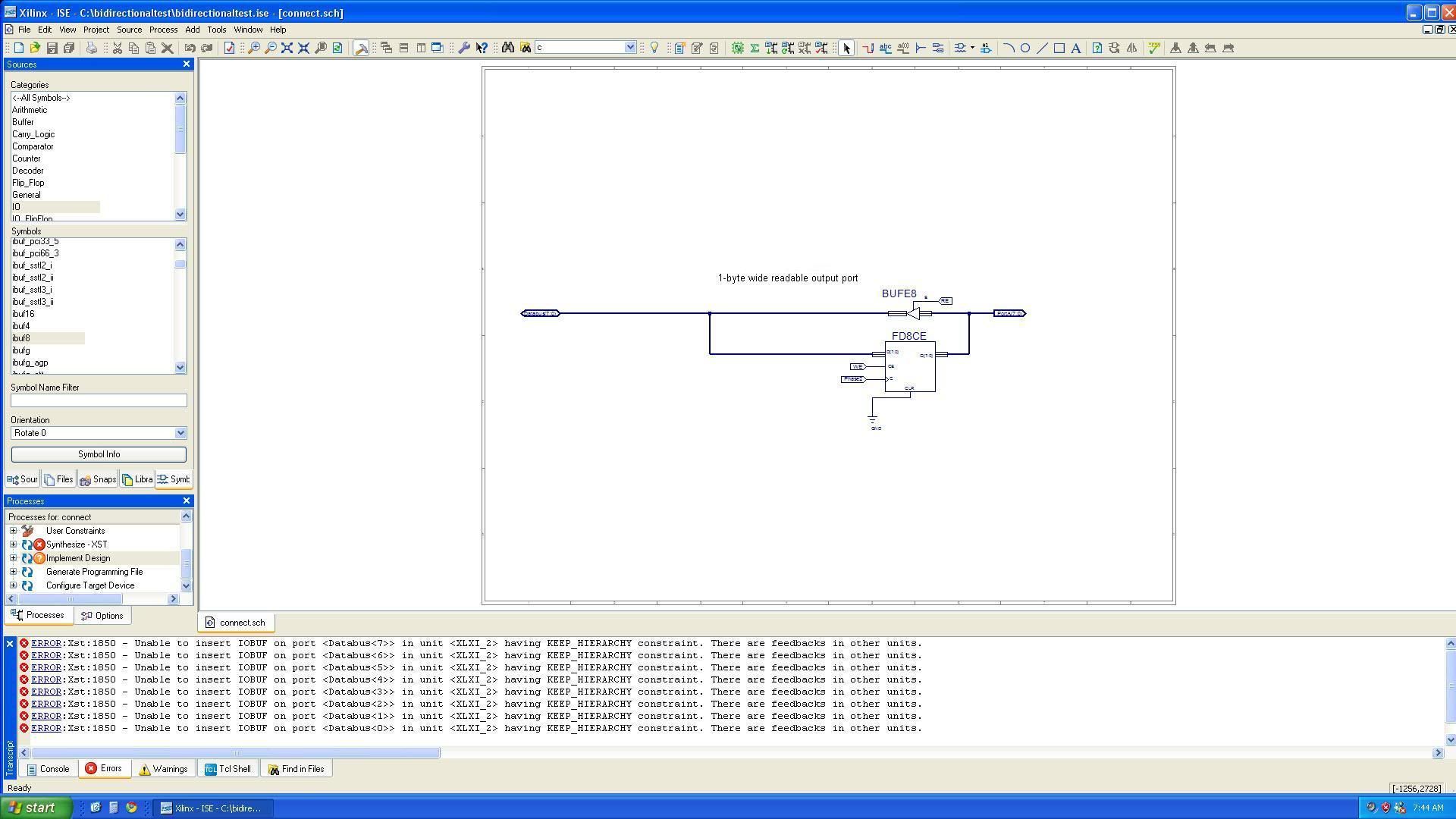
The simple answer is: The ISE software automatically assigns I/O pins based on your schematic/VHDL/Verilog/netlist source.
So you work with ISE to design FIRST, then observe ISE's pin assignments, and then wire it up! Afterwards, you can lock your pins in ISE, so you won't have to rewire your design.
Realize though, once a design expands to a certain level, you may start to observe errors in ISE. If this happens, unlock all pins and see if your design will re-"fit" with the current IC. If you're still having errors, try fitting for a larger device and/or "Clean UP Project Files" under the Project Menu of ISE...
Back to the basics though!
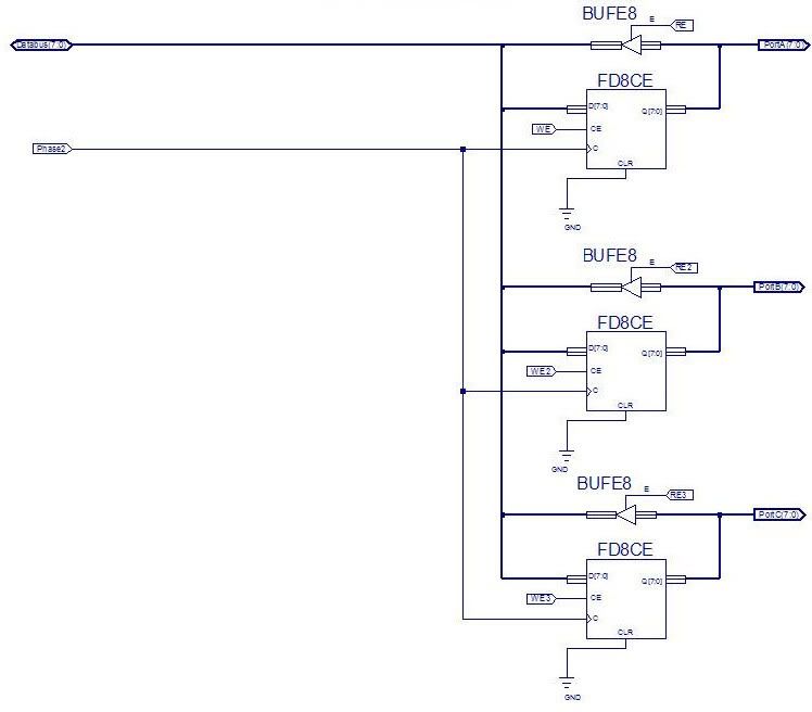
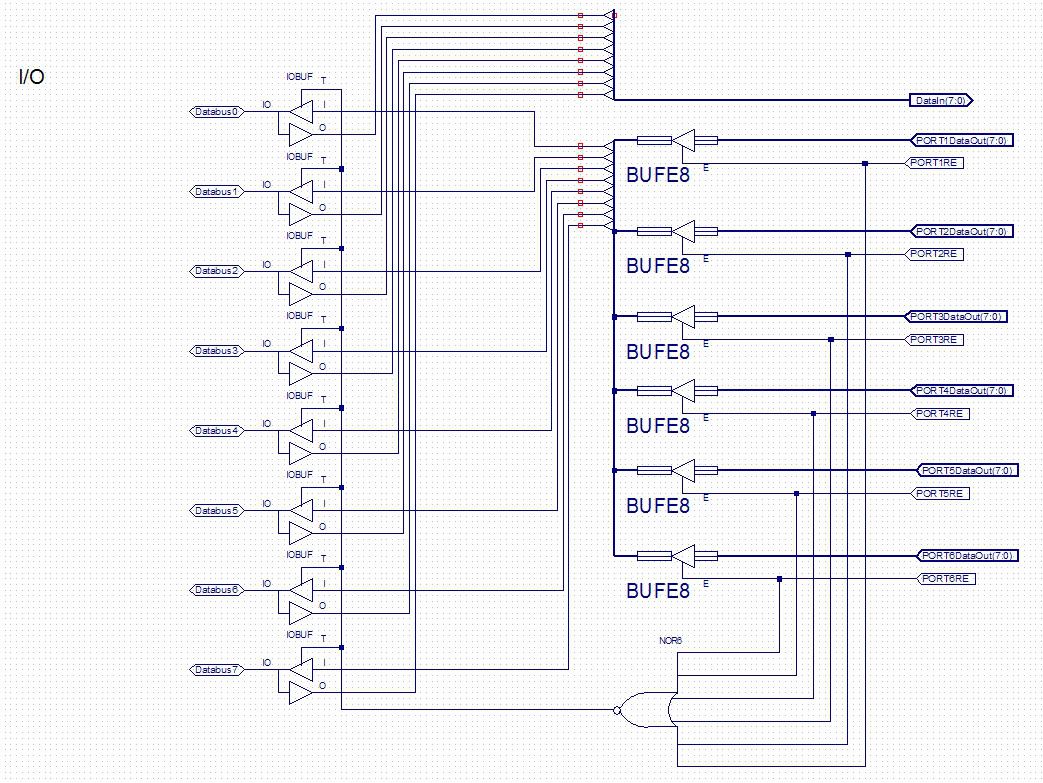
Let's say you need an address decoding circuit. A Xilinx XC9536 ( http://www.xilinx.com/support/documenta ... /ds064.pdf ) would be an excellent choice as it is the smallest of the Xilinx family. It has 5V I/O, 5ns speed, and comes in a 44-pin PLCC. Easy to find a socket for those. (Although, last time I checked DigiKey, only the 10ns version was available in PLCC. Price ~$4US each). Imagine!, you have 34 I/O pins to assign... No problem using all 16 (or more) address lines from a 6502, for a complete "no waste" memory address decode. And don't worry about delays. I've used up to 3 gates in series and have not observed a "summation" of prop delays associated with each gate like one would expect using TTL. Another beauty? Check out the library of gates you get to choose from!: http://www.xilinx.com/itp/xilinx10/book ... ll_scm.pdf
Now, let's say you have your socket and your CPLD. What next?
You will also need a 6-pin male SIP header. Call it the JTAG header.
Next, you will need a JTAG cable.
You can get one from Digilent for $12US. It uses a PC parallel port and will work with many different voltages (1.8V and up) required by various CPLD's/FPGA's. USB versions are a little more expensive ~$50.
Digilent also sells the JTAG header for $1. On the end of the cable is printed the JTAG pin assignments so there's no confusion. http://www.digilentinc.com/Products/Cat ... ,395&Cat=5
We're almost ready. The final piece of the puzzle is the ISE software, and it's free. It's a large download @4GB+, so start downloading it NOW!
We've spent so far, minus shipping: $4 CPLD, $1 PLCC socket, $1 JTAG header, $12 JTAG cable. $1 bypass cap's. <$20 is not too bad ?
Now, to complete the 1st "JUMP".
Wire up all your power connections to the CPLD according to the datasheet and be sure to include include bypass capacitors.
Wire the JTAG header to the CPLD.
Plug in your JTAG cable to your PC and connect it to your header.
Apply power to the CPLD.
Now run the Xilinx Impact program. Right click in the middle of the screen and choose "initiate chain".
If you've done everything correct, ISE Impact will recognize the XC9536.
You are now ready for your second JUMP. Design using the main ISE program!
Previous knowledge of basic TTL/CMOS logic design is assumed.
If you are ready to get your "feet wet" using programmable logic arrays and are starting a new project, forget ABT, ACT, & F series TTL!
Join this CPLD/FPGA revolution and you will understand why it's becoming more and more difficult to find these older discrete devices.
Your journey will be similar to crossing a river by hopping from stone to stone. Sometimes the jumps are quick. Other times, not so quick and you look around and wonder how you got to where you are after so many, many jumps. And then how to make the next jump! One thing I am realizing is that there is no end to crossing the river, it's all about the journey. And forums are a great way to learn!
I'd like to share the little I've learned, in an attempt to learn more.
At the end of this post, you will be ready to make your 1st jump. Good luck!...
I remember looking at my first CPLD Datasheet. It was a Xilinx XC9572 that Daryl was using for his 65SPI controller. Being a regular reader of TTL datasheets, I remember thinking: "How does one go about wiring all the I/O pins?". When reading the CPLD/FPGA datasheet, these pins are just named I/Oxx.
The simple answer is: The ISE software automatically assigns I/O pins based on your schematic/VHDL/Verilog/netlist source.
So you work with ISE to design FIRST, then observe ISE's pin assignments, and then wire it up! Afterwards, you can lock your pins in ISE, so you won't have to rewire your design.
Realize though, once a design expands to a certain level, you may start to observe errors in ISE. If this happens, unlock all pins and see if your design will re-"fit" with the current IC. If you're still having errors, try fitting for a larger device and/or "Clean UP Project Files" under the Project Menu of ISE...
Back to the basics though!
Let's say you need an address decoding circuit. A Xilinx XC9536 ( http://www.xilinx.com/support/documenta ... /ds064.pdf ) would be an excellent choice as it is the smallest of the Xilinx family. It has 5V I/O, 5ns speed, and comes in a 44-pin PLCC. Easy to find a socket for those. (Although, last time I checked DigiKey, only the 10ns version was available in PLCC. Price ~$4US each). Imagine!, you have 34 I/O pins to assign... No problem using all 16 (or more) address lines from a 6502, for a complete "no waste" memory address decode. And don't worry about delays. I've used up to 3 gates in series and have not observed a "summation" of prop delays associated with each gate like one would expect using TTL. Another beauty? Check out the library of gates you get to choose from!: http://www.xilinx.com/itp/xilinx10/book ... ll_scm.pdf
Now, let's say you have your socket and your CPLD. What next?
You will also need a 6-pin male SIP header. Call it the JTAG header.
Next, you will need a JTAG cable.
You can get one from Digilent for $12US. It uses a PC parallel port and will work with many different voltages (1.8V and up) required by various CPLD's/FPGA's. USB versions are a little more expensive ~$50.
Digilent also sells the JTAG header for $1. On the end of the cable is printed the JTAG pin assignments so there's no confusion. http://www.digilentinc.com/Products/Cat ... ,395&Cat=5
We're almost ready. The final piece of the puzzle is the ISE software, and it's free. It's a large download @4GB+, so start downloading it NOW!
We've spent so far, minus shipping: $4 CPLD, $1 PLCC socket, $1 JTAG header, $12 JTAG cable. $1 bypass cap's. <$20 is not too bad ?
Now, to complete the 1st "JUMP".
Wire up all your power connections to the CPLD according to the datasheet and be sure to include include bypass capacitors.
Wire the JTAG header to the CPLD.
Plug in your JTAG cable to your PC and connect it to your header.
Apply power to the CPLD.
Now run the Xilinx Impact program. Right click in the middle of the screen and choose "initiate chain".
If you've done everything correct, ISE Impact will recognize the XC9536.
You are now ready for your second JUMP. Design using the main ISE program!