Page 1 of 2
open source TUBE interface project
Posted: Tue May 18, 2010 6:42 pm
by BigEd
Those following our adventures with BBC micros and CPLDs might be interested in our
latest results with FPGAs.
We (myself and
richarde) have a
couple of FPGA modules from
OHO. The 24-pin module is more capable (has on-board RAM) but the 40-pin is a good device for testing designs.
I loaded the
T65 free 6502 design and got some 6502-like activity on the pins, but it didn't boot in the Beeb and I haven't investigated yet. It could easily be timing problems because I wasn't at all careful with timing constraints.
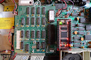
RichardE did much better: he's written a
TUBE in verilog, and after a few iterations it came to life. We've only tried it in a single board: the internal second processor board of his BBC Master. There are pictures in our gallery:
]
We need to try some file i/o, which means finding and hooking up a disk drive: Elite would be a good test! We know the performance will be a few percent off because it's a minimal design with less buffering than the original.
Also, somehow, we'd like to see how this design works in other second-processor hardware. Perhaps we can borrow something.
(Other people have done this before, and there are
one or
two products which include TUBE implementations, but we don't think anyone has released sources.)
Posted: Wed May 19, 2010 3:23 pm
by ElEctric_EyE
Are you able to fit the normal addressable 64K onto the FPGA itself?
Posted: Wed May 19, 2010 6:38 pm
by BigEd
Are you able to fit the normal addressable 64K onto the FPGA itself?
No - the FPGA is a xilinx xc3s250e which has 24kbyte of block RAM - that's 9-bit bytes, if it helps!
It's also possible to use some of the logic fabric as a so-called distributed RAM, but that doesn't seem to be able to give even 8kbyte.
So, this 40-pin part can't be a self-contained 8bit machine with a fully populated RAM. We'll probably have a go with 16k or 24kbyte, to bring up a TUBE+T65+RAM+bootstrap ROM.
(Another idea is to use some RAM as cache, even with a static mapping over zero page and the stack it might be interesting, or perhaps over some interesting part of OS or application code. We're told that FPGAs aren't terribly good at implementing cache - but that might only mean that the size or speed is reduced.)
But the next logical step (for us) will be to move to the 24-pin part which has 512kbyte on-board SRAM. With the RAM on-board, we don't need so many pins to make an interesting system: the host side of the TUBE is only 16 signals or so.
(It might be that the logic fabric can efficiently implement a useful size of ROM - that would be another experiment. We only need 2k or so to bootstrap.)
Posted: Fri May 21, 2010 2:19 am
by ElEctric_EyE
Big Ed, in your post about Dennis Kuschel's WIP, where he uses an XC3S400:
viewtopic.php?t=1544&postdays=0&postorder=asc&start=30, there may be more of a possibility for more onchip SRAM. Unfortunately it looks like there would be alot of unused pins as well. He used the 144 pins version, which I was unable to find in small quantities, a month or two ago. I was able to get the 208 pin version, which I would like to experiment with towards the end of the year after completing the PW analyzer.
Anyway, excellent news about you guys fitting the T65 core onto a Spartan IC. Was it as easy as you make it sound on your site?
Posted: Fri May 21, 2010 7:23 am
by BigEd
Hi EE
yes, putting the T65 onto the FPGA module was very easy - I've got the benefit of some scripts to make everything straightforward - I'm sure we can release those with the rest of the code in a couple of weeks time. Getting it to work is a slightly different question, and I'm not quite there yet. But others have done it, so that's not worrying.
I'd forgotten about Dennis' MyCPU, so thanks for the reminder. The nature of FPGAs is that they do come in impressively large sizes, which is good, but generally with ever-increasing pin counts, which is a mixed blessing. For my purposes, using the commercial modules, I don't get a completely free choice - but then I've also avoided having to deal with multiple power supplies, level converters and high-density surface mount.
There's a table in this PDF
http://www.xilinx.com/publications/matr ... _color.pdf showing how much block RAM is in each part: they are 2kbytes each, so you'd want 32 for a full 64kRAM. That said, you could make up some shortfall using distributed RAM, and also you could wire up sets of 8 RAMs to make 9 byte-wide memories, using all 9 bits width.
(I'll probably be away from the keyboard for a week and a half)
Cheers
Ed
open-source tube source release
Posted: Fri Jun 11, 2010 8:52 am
by BigEd
We've made our first release: see
here.
It's not size-optimised but it does work: the default build uses about 80% of a XC95288 but just 5% of a 3s250 FPGA. (Our main interest is in using it in an integrated design, not in making a low-cost standalone replacement.)
We've included the verilog sources and a python script to drive the Xilinx tools from the linux command line. You'll need your own
FPGA module! (Sorry, this release contains no schematics or block diagram, no Xilinx project file, no FPGA bitstream.)
(Anyone who just needs a replacement Tube chip should consider buying a used one from
Sprow or buying one of
John Kortink's Retula modules.)
We're continuing experiments with the T65 but haven't yet got a bootable design.
Posted: Wed Jun 16, 2010 2:18 pm
by ElEctric_EyE
...It's not size-optimised but it does work: the default build uses about 80% of a XC95288 but just 5% of a 3s250 FPGA...
I've seen a similar pattern, in my project, when migrating from Xilinx's CPLD's to their FPGA's. Their FPGA's are much more adept. However, their CoolRunner series of CPLD's are a good match for something in-between an XC95xxx and an FPGA. Might be worth looking into, if your nearly completed design is only taking up 5%...
In your situation though, the XC95288 is 5V I/O and the Spartan 3 is only 3.3V? How are you dealing with voltage levels?
Posted: Wed Jun 16, 2010 6:31 pm
by BigEd
In your situation though, the XC95288 is 5V I/O and the Spartan 3 is only 3.3V? How are you dealing with voltage levels?
All by the magic of the
OHO modules - it's a 5v FPGA on a 40-pin DIL module. Which also means we don't have to get involved in SMD soldering (yet)
Posted: Fri Jun 18, 2010 11:34 pm
by ElEctric_EyE
I was thinking past few days about your post, and it just struck me about 10 min's ago after coming home from work... Are you saying you fit the T65 core onto an XC95288?!
Posted: Sun Jun 20, 2010 10:07 pm
by ElEctric_EyE
Thinking about it again, there's no way to do that unless you use an external EEPROM/FLASH for the microcode...
Posted: Mon Jun 21, 2010 9:22 am
by BigEd
That's right: this project is FPGA based, not CPLD based.
In other news, we visited the
Vintage Computer Festival at
Bletchley Park at the weekend, and were able to try out our Tube design in a couple of different external second processors connected to a
Master. It turns out not to work, but we did receive a kind donation of a
Z80 second processor, so we'll see if we can come up with a fix.
Probably the problem is at the electrical level, although it could be a timing problem. A couple of knowledgeable people offered the diagnosis that the level-shifters on our board might not interoperate with the databus on the Beeb, which according to the widely circulated
schematic has resistive pulldowns. Our board can write to the host - we know that because we see the startup message - but it may be that the host cannot write to the board.
Posted: Sat Jun 26, 2010 8:54 pm
by Ruud
All by the magic of the
OHO modules - it's a 5v FPGA on a 40-pin DIL module. Which also means we don't have to get involved in SMD soldering (yet)
I I just ordered the 50 pins version (I think I can use the extra pins for future use). I always wanted to play with FPGA, see my "6502 in FPGA" threat. Now I have the chance! (thanks to my lovely wife)
But having almost no experience with Verilog or VHDL I want to use the code of your BBC project as base. My first goal is to make it run on a VIC-20 (what else? :) I hope I can ask you for advice in case of trouble.
Posted: Sat Jun 26, 2010 9:19 pm
by BigEd
Excellent! The more 6502 fans with FPGA tooling, the better!
We've made just a little progress with our experiments. It turns out that there are three types of Tube interface with differences which might be crucial.
We are getting some success with donor Tom's Z80 second processor, in the case of using the Tube interface on a Model B. In this case, the Tube databus is actually the CPU databus, which can have quite a lot of other loads on it. Actually, our device works with the original CPU, but not with a 65816 replacement.
Our lack of success at the VCF was with the external Tube interface on a Master, which is almost an isolated bus - the CPU databus is bridged through a custom part called the PBC.
We may have some logic problems, but it looks likely that we have interface or timing problems, so...
I rescued my very old oscilloscope from the garage, and got some traces displayed. It uses 100w, and in the current weather I can only really use it in the morning - the room gets too hot later in the day. I was lucky enough not to have lost the probes - as it is, only one has a ground clip, so the clock waveform is probably affected by a bad ground:
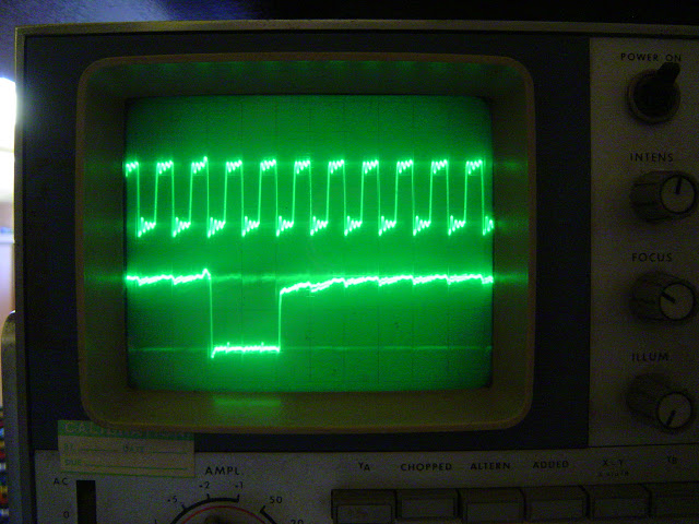
No debug yet, but some capability for debug.
Posted: Sun Jun 27, 2010 4:09 am
by BigEd
I just ordered the 50 pins version (I think I can use the extra pins for future use). I always wanted to play with FPGA, see my "6502 in FPGA" threat. Now I have the chance! (thanks to my lovely wife)
But having almost no experience with Verilog or VHDL I want to use the code of your BBC project as base. My first goal is to make it run on a VIC-20 (what else? :) I hope I can ask you for advice in case of trouble.
Yes, of course! (Sorry, should have answered this question instead of going off on a tangent about my 'scope)
Posted: Tue Jul 13, 2010 7:50 am
by Ruud
Hallo BigEd,
Next week my holidays will start and then I have time to focus on the GODIL module. My problem: I have no experience at all with FPGA's and Verilog and just a bit with VHDL and CPLD's. What I need is a kind of "GODIL for dummys" that enables an intelligent dummy like me to start up his first Verilog or VHDL program. IMHO something simple like reading the buttons and flashing the onboards LEDs is fine for me. URLs or other sources for learning Verilog are fine as well. In short: anything that helps me starting up the project.
How did you start up? I cannot imagine that you took the GODIL out the box, connected it to a programmer and things worked like a charm from the first moment on. A step-by-step guideline how you did it could already do the trick. BTW, I haven't any idea what you use to program the GODIL but FYI, I ordered this USB-JTAG cable. And what software are you using? I presume the ISE Webpack but just to be sure.
One thing is already confusing me: I know you connect a CPLD directly to a JTAG cable. But in this case the GODIL has these extra IC's, AFAIK the EEPROMs (or whatever) that fill the FPGA with data at start-up. But how are these EEPROMs filed? And what makes the EEPROMs to fill the FPGA with data? Is that something already present inside the FPGA? Maybe it is as simple as "ignore it and treat the whole as a CPLD" using your JTAG cable but at this moment I haven't any idea.
I did RTFM the GODIL PDF but IMHO it wasn't that helpfull.
I can imagine that other readers consider this as OT so you can answer me by email (as well): ruud (at) baltissen.org
At the end of next week I'm going to Poland and I would appreciate it having some answers by then as my mother-in-law hasn't an Internet connection.
Thank you very much!