Page 1 of 1
On 6502 undocumented opcodes in hardware-level detail...
Posted: Thu Oct 30, 2008 5:55 am
by kc5tja
Recently, I came across a positively
fascinating article:
http://www.pagetable.com/?p=39
thought others here would really enjoy this.
Posted: Mon Nov 03, 2008 3:59 pm
by schidester
Thank you, that is an interesting article, and pretty much affirms what I thought was happening (at a basic level at least). I'd suspect that the combination arithmetic/shift instructions are caused by the same phenomenon... that the PLA is generating control signals for the ALU and shift registers at the same time.
6502 alu
Posted: Sun Jul 12, 2009 4:01 pm
by BigEd
That pagetable article is excellent. Somewhere I've seen a good description of the transistor-level (switch-level) design of the 6502 ALU, but I can't find it. But I did find
this page (now
here) with a reverse-engineered diagram of (some of) the NMOS 6502 ALU:

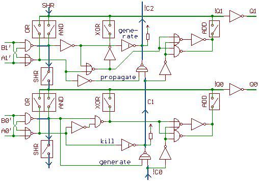
(Edit: I now see there's a similar diagram of this in patent 3991307 - pdf available
here)
I haven't figured out the difference between the two bit-slices. (Edit: aha, it's the inversion of carry out in alternate bits, presumably to simplify the implementation.)
On the subject of implementations (and side-effects)
this page goes into a little detail about how BRK, RTI, JSR and RTS share the same sequence.
There's more detail in Bill Mensch's patents - see the "description of the invention" in
here for example. Surprisingly readable for a patent - even covering the design decisions.
Edit: updated image URL
Posted: Mon Jul 13, 2009 2:19 pm
by Nightmaretony
Ah, Jed Margolin's website. Traipse around it, plenty of fun things. Had emailed with him for a bit concerning a game of his called Hard Drivin.
The internal emails of Atari in those years are fascinating to no end
