Page 1 of 1
Chip photo
Posted: Tue Jun 24, 2003 2:17 pm
by schidester
Just for fun, check out:
http://micro.magnet.fsu.edu/chipshots/m ... large.html
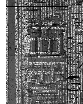
Now, does anybody know which sections are which? My best guesses are that the yellow area with 16 pads on it is the address buffer, the red area around the opposite edge is the data bus with some control lines, the green rectangle at the bottom is for some registers, the area at the top is the ALU with perhaps the accumulator register, and the area in the center is the control unit. I'm also guessing that the small three cyan rectangles on the right are the sequencer for the control unit, to provide up to eight cycles for an instruction.
Anybody have any better guesses?
Posted: Wed Aug 10, 2005 2:55 pm
by debounce
I'm guessing the green rectangle is the microcode array. Microcoded CPUs don't necessarily need instruction counters, as each row (vertical in the photo) can select the next one to be activated, in linked-list fashion (optimised for sequential walking or jumps to a small number of entry points) and the instruction is done when it's done.
The eight long processes under the yellow address pads would be the bit slices of the ALU. Where the registers are is unclear from the photo - perhaps embedded in the ALU or fitted in spare corners (any 8x repeated feature is a candidate.)
Posted: Wed Aug 10, 2005 4:35 pm
by kc5tja
I'm guessing the green rectangle is the microcode array.
Except the MOS 6502 is known not to employ microcode -- it is a pure hardware design, like many RISC processors (this, in conjunction with its exceptional performance, even once got the 6502 erroneously branded as the world's first RISC). Several references do mention that the 6502's address decoder is built on a PLA -- this could be the AND-matrix of the PLA, with that random mish-mash above it being, at least partially, the OR-matrix.
The eight long processes under the yellow address pads would be the bit slices of the ALU. Where the registers are is unclear from the photo - perhaps embedded in the ALU or fitted in spare corners (any 8x repeated feature is a candidate.)
I hadn't seen these features before you pointed them out to me. I have to agree, and it makes sense that the ALU is sitting right next to at least one of the address buffers, since the ALU is used heavily for address calculations. I also feel that the registered are embedded right into the ALU as well.
Posted: Thu Aug 11, 2005 2:43 pm
by debounce
Except the MOS 6502 is known not to employ microcode -- it is a pure hardware design, like many RISC processors
Which only increases my astonishment at the chip

The 6502 being CISC in so many ways, I'd assumed microcode came with the territory. Given the complexity of some instructions, you'd be forgiven for thinking so...
Posted: Fri Aug 12, 2005 7:45 am
by BitWise
The image is similiar to figure 2 in Bill Mensch's IC Topography patent (4,652,992) - but upside down.
Assuming his patent is a refinement of ideas he started with on the MOS 6502 then.
The pins on the top of the left side would be the data bus.
The top pads are the high order address bus
The pins on the top of the right side are the low order address bus
The registers the blueish region at the top (and run horizontally)
The central redish area is the RTL and sum of miniterms
The green section are the miniterms
The pads around the lower half are timing comtrol and interrupts
Posted: Fri Sep 01, 2006 11:28 pm
by pet1978
There is a Hungarian website that has a very high-resolution image of the 6502 die. The fellow has also reverse engineered a schematic diagram of the actual 6502 circuitry.
http://impulzus.sch.bme.hu/6502/6502/
The schematic and high-resolution image are at:
http://impulzus.sch.bme.hu/6502/letolt.php3
Posted: Fri Sep 01, 2006 11:53 pm
by kc5tja
WOW, thanks!
Now if only I could understand the Hungarian language. The schematic is pretty big too. I was expecting someone to actually reduce the transistors to logic gates, where it'd be a bit more meaningful. At least the raw data is there though.
Now, where did I put all my *time*?
Posted: Thu Oct 05, 2006 2:39 pm
by schidester
That's a little more detail than the original shot I found!
Posted: Thu Mar 15, 2007 8:21 pm
by pet1978
Here is a link to a promotional video by Commodore Germany. About 3 minutes in, they take you on a 15 minute tour of the MOS Technologies semiconductor facility in Norristown, PA. The video shows the Commodore 64 VIC-II chip being made, but this would be the same process as the 6502.
http://video.google.com/videoplay?docid ... 8384520969
Re: Chip photo
Posted: Fri Dec 25, 2009 12:21 pm
by BigEd
Just for fun ... I'm also guessing that the small three cyan rectangles on the right are the sequencer for the control unit, to provide up to eight cycles for an instruction.
Just for fun, I had a good look at that area. In fact it holds 8 large inverters - looks like the databus being driven into the instruction pre-decode (*). As the outputs go immediately through some pass transistors (clocked by phi2) I'm not sure why they are so large. According to the giant schematic, the sequencer is just to the right of this structure, in the photomicrograph, or just to the left in the image you posted.
Here are the three cyan rectangles, on the right edge:
Here's the same structure on the left of Beregnyei Balazs' photomicrograph:
- 6502detailmicrophoto.png (12.21 KiB) Viewed 4002 times
Here it is full size (note that it is distorted - Y axis is larger scale than X):
And here I've highlighted two of the inverters, with the following pass gate, and a little of the VSS net:
(I'm not endorsing MSpaint as a layout tool.)
Here's the corresponding left edge of the circuit diagram:
Edit: (*) But I don't see D4 and D7 being taken off from the inverters before the pass gates, as shown in the schematic. I'm tempted to distrust the schematic, but I'm not sure what's going on. Is it even safe to take unclocked signals north into that cloud of logic whose output is latched on PHI1?
Posted: Wed Sep 08, 2010 9:36 pm
by BigEd
While I was messing about in MSPaint, some rather more capable people were doing a proper job of reverse engineering. I've started a thread
here on that topic.
Posted: Mon Sep 27, 2010 12:00 am
by RichCini
Here is a link to a promotional video by Commodore Germany. About 3 minutes in, they take you on a 15 minute tour of the MOS Technologies semiconductor facility in Norristown, PA. The video shows the Commodore 64 VIC-II chip being made, but this would be the same process as the 6502.
http://video.google.com/videoplay?docid ... 8384520969
This is a great video. Although I wish I spoke German, it's pretty understandable. According to Wikipedia, it's a "circa 1970 one micrometre plant". It says earlier that it was opened in 1969 by Allen-Bradley (I knew the A-B connection but not the year).
Given that, it is still amazing how primitive the production facility looks and how they were able to turn out working chips from the plant. I wonder what the production capacity of the plant was? I saw a reference to 10,000 5" wafers per month but I don't know how many dice were on each wafer.
EDIT1: transistor count quoted as 3,510 on a 21mm-sq die size. The 21mm doesn't seem right -- that's 0.83". The same table from the Microprocessor Report shows the 6800 at 16mm-sq (0.63") and the transistor counts are very similar.
EDIT2: I don't know if 1um is the right process. Contemporary processors like the 4004/8008 (slightly earlier) used a 10um process. The 8080 was 6um. In the entry I read on Wikipedia, 1um was used on the 80486 in the late 1980's. So, something's not right. Maybe just a typo...
Ah, memories. Maybe I'll drive by the plant again someday -- last time was in 1997/1998.
Posted: Mon Sep 27, 2010 4:02 am
by GARTHWILSON
EDIT1: transistor count quoted as 3,510 on a 21mm-sq die size. The 21mm doesn't seem right -- that's 0.83".
21 square mm makes more sense. If it were square, that would be about 4.6mm square.
Posted: Mon Sep 27, 2010 12:06 pm
by RichCini
EDIT1: transistor count quoted as 3,510 on a 21mm-sq die size. The 21mm doesn't seem right -- that's 0.83".
21 square mm makes more sense. If it were square, that would be about 4.6mm square.
Agreed. The column heading must be mislabeled and I wasn't thinking about transposing the units. The column in this particular article should probably be "die area" rather than just "die size".