Re: "Fast" PDIP 6502 design feedback
Posted: Wed Aug 23, 2023 11:52 pm
I have been playing with serial circuits, and made quite a compact one to hook up to the prototype:
The oscilloscope shows receiving a signal (yellow), reconstructing the clock for it (blue), signalling the end of the byte (red), and the user code responding by echoing the characters back (green).
It was quite awkward to hook up to the PCB prototype, but it is working fairly well. One constraint of this circuit is that it has to run at quite fast speeds - I think 125000 baud is currently the slowest it can go, I currently have it set to 250000 though. This is due to dividing an 8MHz clock, and needing to be able to count time across a whole byte within 10 counter bits.
Some of the behaviour is based on my vague recollections of how the 6850 worked. The circuit provides a 1-byte read FIFO (so you have about one byte's duration of time in which to read the previous byte) but no transmit FIFO, you have to wait for the previous byte to fiinsh before sending the next one, and this is leading to longer stop bits in the green trace above as the transmit line is idle while the CPU gets the next character ready.
It has TDRE and RDRF flags (transmit data register empty, receive data register full), which are cleared by sending a new byte or reading the received byte respectively, and it requests interrupts when these are first set; in case you have finished transmitting data and don't want to send more, you can clear the interrupt without sending a new byte as well. It was designed on paper, but turned out quite nice to code for, and works well with either polling or interrupt-driven code.
I wanted to include a receive overflow flag, and a receive framing error flag, but instead used those resources to divide the clock and allow slightly slower baud rates. I may backtrack on that though and require faster rates instead, or just add another counter to divide the receive clock, as these flags are pretty nice to have.
The circuit is just two counter ICs for timing the signals, a shift register for receives, and two ATF22V10 PLDs. I don't like using these PLDs because they use a lot of power (relative to everything else, anyway) and get quite warm - but features like individually enablable outputs were useful for providing a status register, and I have a few to use up, these parts are all ones I already had.
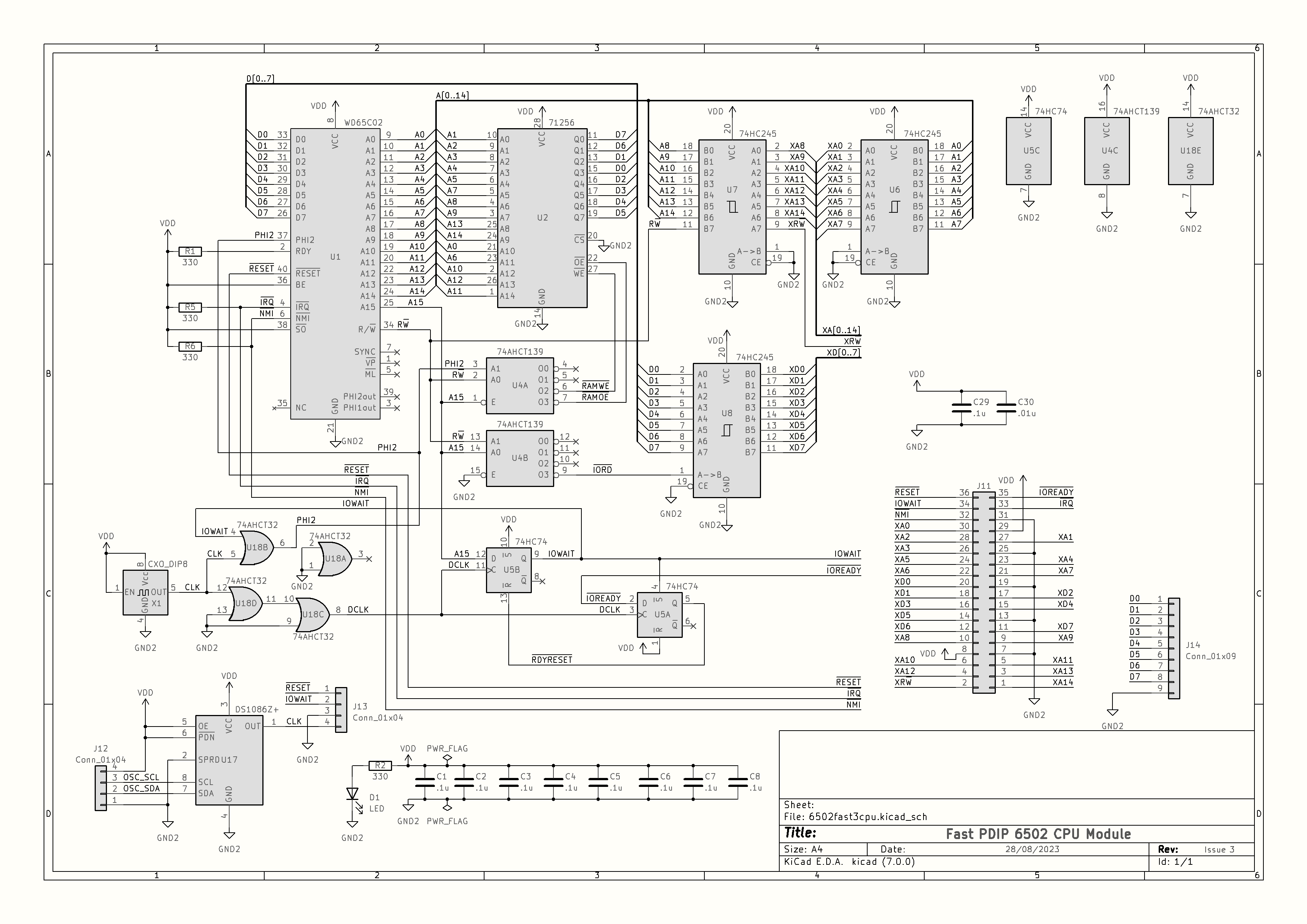
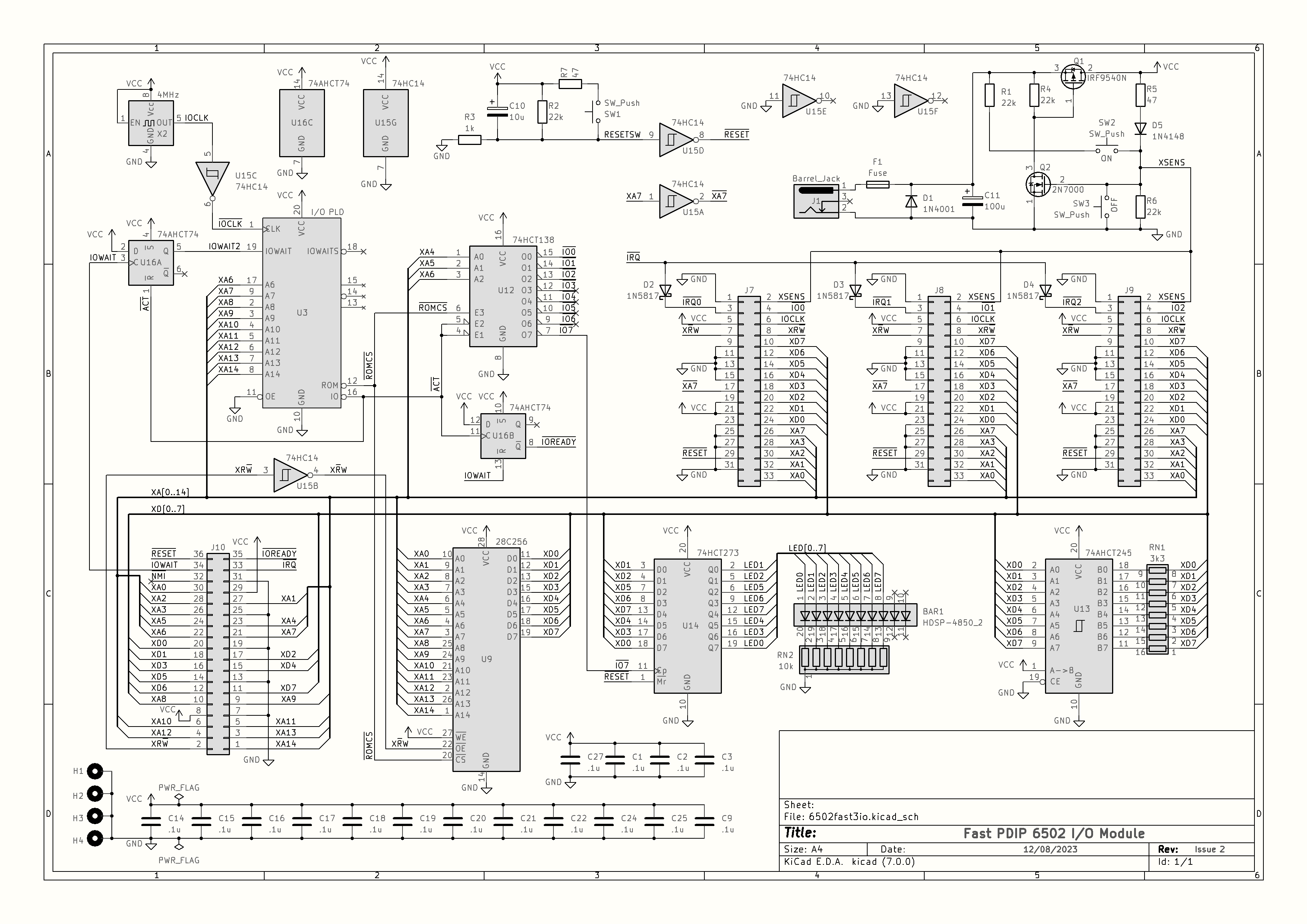
That bit is not exactly 6502-related, but if anyone is interested in more details about the circuit (the schematic, the PLD code) then let me know and I can share those.
It was quite awkward to hook up to the PCB-based prototype. I couldn't get pin clips to actually grab the pins I needed, and with the weird shape of this prototype at the moment (CPU mounted on the back) it was tricky. Then I realised I could use the VIA board I'd already made, but without a VIA in it, and stick the wires into the IC socket in there, which worked fairly well. I ought to solder up another copy of this but with pin headers or dupont sockets instead of the IC socket, to make this easier. The idea was really to prove out the circuit so that I can get a PCB made for it and be confidennt it will work - it doesn't have to run like this in the long term.
The biggest difficulty with this whole thing was discovering that when I mounted the second CPU socket on the back of the board I had failed to connect the RWB pin - this wasn't noticeable until now, because with the pin disconnected it was defaulting to reads, which was fine for the ROM, and my debug port also doesn't care about RWB. It took quite a while to deduce what was wrong - the main symptom was the IRQ line getting stuck active, as it's only cleared by writing to the status register, and my board wasn't able to detect any writes. It was fairly easy to resolder that pin though, and worked straight away after that. I was also glad the issue was in the bodge rather than a flaw with the design.
Another issue I've been having is with the FTDI serial adaptor - the ground level coming from there is not the same as that from my USB power supply. Sometimes it works well with the grounds directly connected, other times not. I don't know what the right approach is - for now I have connected the GND, RX, and TX pins through small resistors (47 ohms I think) and also bridged the RX and TX to ground through somewhat larger resistors - this seems to be OK and behaves more consistently. I also tried powering the whole circuit from the FTDI adaptor's +5V line, but it droops to about 4.6V so I'm not keen to do that really.
I'd be interested to hear what proper solutions are for this grounding issue - is it wrong to connect these grounds together, does it ultimately need optocoupling or something like that? Surely not, as serial links have been used for decades... What about capacitative decoupling, a high-pass filter of sorts, biased to settle at +5V? It feels like that could work well.
It was quite awkward to hook up to the PCB prototype, but it is working fairly well. One constraint of this circuit is that it has to run at quite fast speeds - I think 125000 baud is currently the slowest it can go, I currently have it set to 250000 though. This is due to dividing an 8MHz clock, and needing to be able to count time across a whole byte within 10 counter bits.
Some of the behaviour is based on my vague recollections of how the 6850 worked. The circuit provides a 1-byte read FIFO (so you have about one byte's duration of time in which to read the previous byte) but no transmit FIFO, you have to wait for the previous byte to fiinsh before sending the next one, and this is leading to longer stop bits in the green trace above as the transmit line is idle while the CPU gets the next character ready.
It has TDRE and RDRF flags (transmit data register empty, receive data register full), which are cleared by sending a new byte or reading the received byte respectively, and it requests interrupts when these are first set; in case you have finished transmitting data and don't want to send more, you can clear the interrupt without sending a new byte as well. It was designed on paper, but turned out quite nice to code for, and works well with either polling or interrupt-driven code.
I wanted to include a receive overflow flag, and a receive framing error flag, but instead used those resources to divide the clock and allow slightly slower baud rates. I may backtrack on that though and require faster rates instead, or just add another counter to divide the receive clock, as these flags are pretty nice to have.
The circuit is just two counter ICs for timing the signals, a shift register for receives, and two ATF22V10 PLDs. I don't like using these PLDs because they use a lot of power (relative to everything else, anyway) and get quite warm - but features like individually enablable outputs were useful for providing a status register, and I have a few to use up, these parts are all ones I already had.
That bit is not exactly 6502-related, but if anyone is interested in more details about the circuit (the schematic, the PLD code) then let me know and I can share those.
It was quite awkward to hook up to the PCB-based prototype. I couldn't get pin clips to actually grab the pins I needed, and with the weird shape of this prototype at the moment (CPU mounted on the back) it was tricky. Then I realised I could use the VIA board I'd already made, but without a VIA in it, and stick the wires into the IC socket in there, which worked fairly well. I ought to solder up another copy of this but with pin headers or dupont sockets instead of the IC socket, to make this easier. The idea was really to prove out the circuit so that I can get a PCB made for it and be confidennt it will work - it doesn't have to run like this in the long term.
The biggest difficulty with this whole thing was discovering that when I mounted the second CPU socket on the back of the board I had failed to connect the RWB pin - this wasn't noticeable until now, because with the pin disconnected it was defaulting to reads, which was fine for the ROM, and my debug port also doesn't care about RWB. It took quite a while to deduce what was wrong - the main symptom was the IRQ line getting stuck active, as it's only cleared by writing to the status register, and my board wasn't able to detect any writes. It was fairly easy to resolder that pin though, and worked straight away after that. I was also glad the issue was in the bodge rather than a flaw with the design.
Another issue I've been having is with the FTDI serial adaptor - the ground level coming from there is not the same as that from my USB power supply. Sometimes it works well with the grounds directly connected, other times not. I don't know what the right approach is - for now I have connected the GND, RX, and TX pins through small resistors (47 ohms I think) and also bridged the RX and TX to ground through somewhat larger resistors - this seems to be OK and behaves more consistently. I also tried powering the whole circuit from the FTDI adaptor's +5V line, but it droops to about 4.6V so I'm not keen to do that really.
I'd be interested to hear what proper solutions are for this grounding issue - is it wrong to connect these grounds together, does it ultimately need optocoupling or something like that? Surely not, as serial links have been used for decades... What about capacitative decoupling, a high-pass filter of sorts, biased to settle at +5V? It feels like that could work well.