Page 6 of 6
Posted: Thu Oct 14, 2010 6:11 am
by GARTHWILSON
I don't have any numbers, but consider this: the "plate width" of adjacent edge fingers is actually the copper thickness, which is only a couple of mils. The dielectric in this case is air with a K of approximately 1. The wider dimension of a finger on one side is opposed to that of a finger on the other side (if present) but has the relatively thick PCB material as the dielectric. Typical PCB construction produces a K of around 4.6.
Another consideration of using edge connections as opposed to pins is if the pin header is on the motherboard (as it appears you are planning)
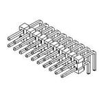
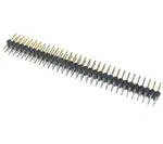
I'm putting the pins on the module, tentatively with a right-angle dual-row pin header with .040" between pads allowing traces to be run between them. It could be either way (ie, put the pins on the computer board or put the socket on it), but the pins, which can be more easily damaged, usually get put on the part that's more easily replaced; so on VME bus for example, the pins go on the boards, and the sockets go on the backplane (even though a computer board could be thousands of dollars <cough, choke>). Fortunately the pin headers are very cheap, and they're quick to solder by hand. The idea is
- 71764a.jpg (4.54 KiB) Viewed 570 times
although I could also go with straight ones and just solder the edge of the board down between the pins on the short side of
- 70280a.jpg (3.77 KiB) Viewed 570 times
then the mating receptacle has to be mounted to the memory module, which might complicate the physical construction. With edge connections, nothing has to be attached to the memory module PCB except the components. With a four-layer module, it should be possible to eliminate decoupling capacitors, since the power and ground planes act as the plates of a large capacitor.
Having parallel planes close together for power and ground, IIRC, eliminates the inductance, so decoupling capacitors should not be needed close to the ICs, as long as you don't run connections right up to the edge of the planes. Ideally the planes are infinite, but staying away from the edge a little becomes a close enough approximation. I would like to find Dr. Howard Johnson's article again where he discusses that though.
I recall the days when memory was sold as SIPs, which plugged into a receptacle on the motherboard. Aside from the ease at which the pins could be broken off a SIP, it was discovered that the receptacle introduced undesirable reactive effects. You don't see SIP memory modules anymore.
I expect it's mostly because of the much higher speeds used today, but also because the number of pins needed would require them to be too small and fragile. IC pins are generally about .015" x .018", which is partly why I decided against making the module like an IC that plugs into an IC socket-- damaging a couple of pins gets a whole lot more expensive for this than for a $6 processor. The .025" square posts are much sturdier.
I'm sure the industry would have stayed with them if it produced better (and less expensive) results. Either way, a receptacle of some kind will be required.
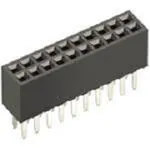
The plan at this point is to put the receptacle on the computer board, similar to this:
- m50-300.jpg (4.68 KiB) Viewed 570 times
which can be cut to any length and is relatively inexpensive.
The module will go perpendicular to the computer board.
I haven't gotten to work on it in a couple of days though. I should make some more progress on it this weekend.
SIMMs for 65xx MPUs
Posted: Thu Oct 14, 2010 4:40 pm
by BigDumbDinosaur
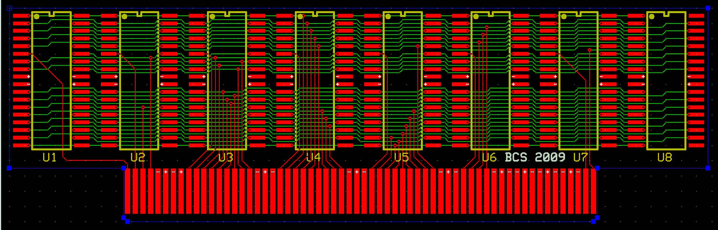
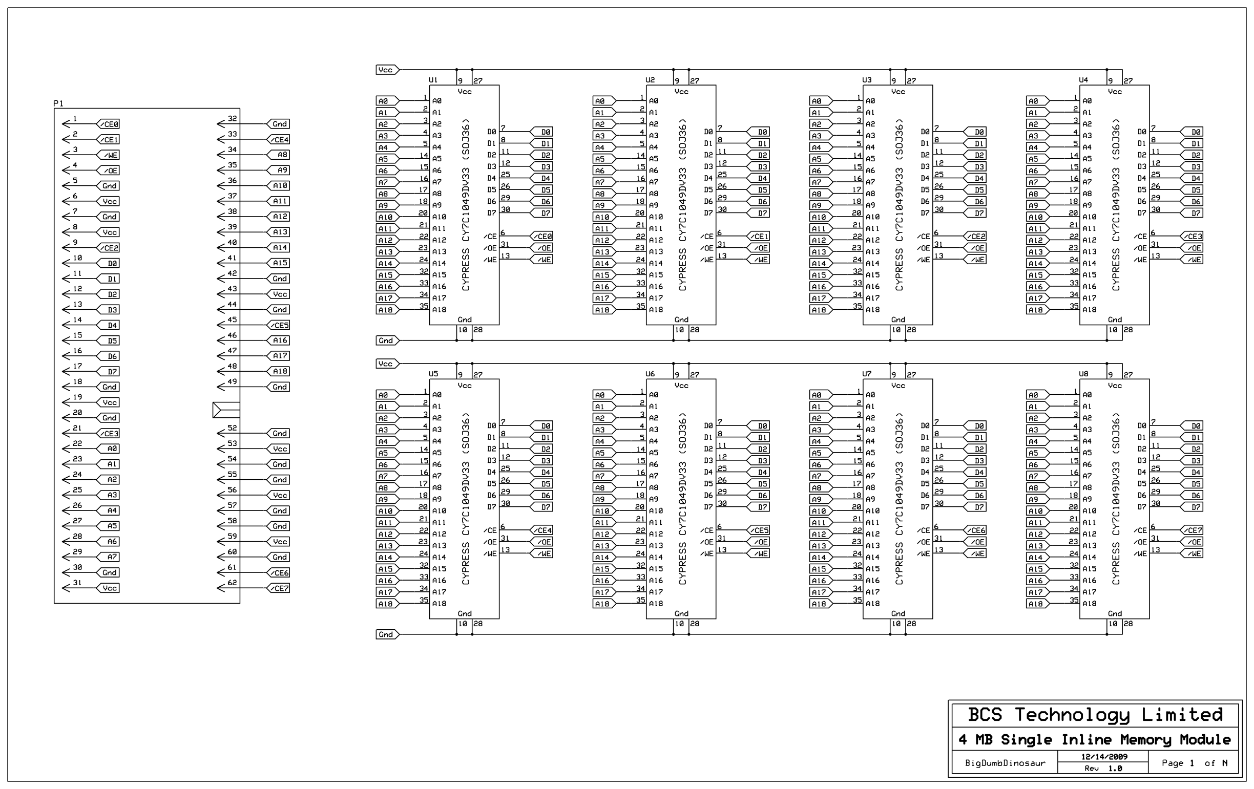
Here's the four-layer version of my 4 MB SIMM. It's a bit smaller than the two-layer version and also fits an industry standard 32 bit PCI socket. The SRAM are SOJ36 packages. Overall length is 4.575 inches, nearly an inch shorter than an industry standard DIMM. BTW, this board can be gotten through EPCB's Proto-Pro four-layer service, despite the routed edges.
Incidentally, because this design is single-sided and can lay flat, it should be possible to fabricate it in a makeshift reflow oven. Were it double-sided, such a procedure would be somewhat problematic, I would think.
Here's the schematic to go with it.
How to fabricate a memory module?
Posted: Thu Oct 14, 2010 4:51 pm
by BigDumbDinosaur
What I missed on first look was that you were not using the contacts on the oposite side of the board. The K of around 4.6 would make for a higher capacitance to them than just air, but you don't have any anyway.
Even if there was an opposing finger, the combination of the two fingers separated by the .06 inch average thickness of the PCB would make for a very poor capacitor.
I'm doing two rows of pins partly because the board is not long enough to do it with a single row with anything that will fit in standard perfboard.
Yeah, length could be an issue with perf board. Also, with all those holes in it, perf board is not as rigid or as resistant to breakage as a typical PCB of the same dimensions. BTW, are you planning to wire-wrap this thing?
Posted: Thu Oct 14, 2010 9:36 pm
by GARTHWILSON
Even if there was an opposing finger, the combination of the two fingers separated by the .06 inch average thickness of the PCB would make for a very poor capacitor.
C=.2235KA/d(N-1)
where:
C=capacitance in pF
K=dielectric constant
A=area of one plate in square inches
d=thickness of the dielectric in inches
n=number of plates
It looks like your board-edge contacts are about .030"x.300", making A .009 sq. in.
d is .06"
N is 2
so C is 0.154pF which is truly negligible in view of the input capacitance of the chips themselves. .025" square posts, having no more area (a little less width but a little more length if I use the 90° ones) but greater separation (.075" instead of .062"), will have even less capacitance if anything. I'm glad you made me go through that exercise. So the capacitance either way is not worth worrying about. I was thinking it was more, because many years ago I needed a small capacitor for an RF application late at night or on a weekend so I made it by cutting a tiny piece of double-sided copper-clad PC board and soldering a lead to each side. It may have been .030" board though and I may have only needed half a pF. I don't remember.
In any case, digital circuits like this are considered low-impedance AC-wise, so the focus on inductance remains, and good layout is imperative.
Incidentally, because this design is single-sided and can lay flat, it should be possible to fabricate it in a makeshift reflow oven. Were it double-sided, such a procedure would be somewhat problematic, I would think.
Pololu will make solderpaste stencils from your gerber file and they're not very expensive either; but solderpaste's shelf life is pretty short which may not be practical for something like this where I may go months between batches. In higher-volume automated production, putting parts on both sides generally involves putting a spot of epoxy on the parts on the bottom and curing it to keep them from falling off in the machine; but I suppose that doing them at home you could solder the parts on one side, then if they're all the same height, put the board up-side-down on an even surface to re-heat it to do the parts on the other side. The solder holding the parts on the first side will melt again, but as long as you don't bump it while it's hot, everything should stay in place. I plan to just solder them by hand though. Doing SOJ's by hand does not require soldering one lead at a time. You just flood the entire side with solder, using a tip that covers two or three leads at once, leaving lots of bridges, then hold it vertically and go from top to bottom again with the iron, and all the excess solder comes off on the iron, leaving an even amount of solder on every pin, just right. It's amazing how easy it is. You need a lot of flux though, then you have to wash the whole gooey mess off. I have an idea for making a small vapor degreaser.
BTW, are you planning to wire-wrap this thing?
No, but I will have to wire-wrap a tester to start, using perfboard with ground plane and maybe power plane too. With plated-thru holes, you can have chip capacitors soldered to the power pins for power-supply bypassing even though it's prototyping perfboard. (It's expensive board, but I have some here.)
Posted: Sun Oct 17, 2010 5:44 am
by digidice
Pretty excited to see how well those ram expander boards work. I wonder if a DIMM socket would be workable? the PCI is solder easy but it does take a bit of real estate. Space matters not to me, I like things I can see and get my hands on. Maybe thats why I like tubes. but thats another topic.
Posted: Sun Oct 17, 2010 6:09 am
by GARTHWILSON
Maybe thats why I like tubes.
 Actually I did work with tubes just a little in my early years.
Pretty excited to see how well those ram expander boards work. I wonder if a DIMM socket would be workable? the PCI is solder easy but it does take a bit of real estate. Space matters not to me, I like things I can see and get my hands on.
I haven't been able to work on the RAM board in several days, but I'm anxious to get back on it. A couple of criteria are that the connectors can be put on common perfboard (it does not look like PCI or DIMM can), and be readily available and relatively inexpensive in small quantities.
Posted: Mon Oct 18, 2010 3:55 am
by BigDumbDinosaur
Maybe thats why I like tubes.
ICs come in tubes!
Actually I did work with tubes just a little in my early years.
I still do...work on tubes. I do the bench work for
Vero Amplifiers.
A couple of criteria are that the connectors can be put on common perfboard (it does not look like PCI or DIMM can), and be readily available and relatively inexpensive in small quantities.
Yeah, perf board is a problem with its .100 x .100 grid.
Posted: Mon Oct 18, 2010 3:58 am
by BigDumbDinosaur
Pretty excited to see how well those ram expander boards work. I wonder if a DIMM socket would be workable? the PCI is solder easy but it does take a bit of real estate. Space matters not to me, I like things I can see and get my hands on. Maybe thats why I like tubes. but thats another topic.
DIMM sockets actually take up more real estate than PCI sockets. Also, DIMM sockets have a lot of pins, far more than are needed for this sort of project/
Posted: Mon Oct 18, 2010 5:17 am
by digidice
Pretty excited to see how well those ram expander boards work. I wonder if a DIMM socket would be workable? the PCI is solder easy but it does take a bit of real estate. Space matters not to me, I like things I can see and get my hands on. Maybe thats why I like tubes. but thats another topic.
DIMM sockets actually take up more real estate than PCI sockets. Also, DIMM sockets have a lot of pins, far more than are needed for this sort of project/
well this is true, Maybe a Simm socket might be a better route, Although I am not sure you can purchase them anymore. Just throwing some ideas out there.
Posted: Mon Oct 18, 2010 3:42 pm
by BigDumbDinosaur
DIMM sockets actually take up more real estate than PCI sockets. Also, DIMM sockets have a lot of pins, far more than are needed for this sort of project.
well this is true, Maybe a Simm socket might be a better route, Although I am not sure you can purchase them anymore. Just throwing some ideas out there.
At one time Jameco had 30 pin SIMM sockets in their catalog. They still list sockets for 72 pin SIMMs. That said, I recommend staying away from sockets intended for use with specific types of obsolete hardware. That was one of the reasons I decided on the 32 bit PCI socket. Those will be around for some time to come due to extensive proliferation. At the bus speeds we use in our homebrew stuff, the insertion loss of the PCI socket is negligible (32 bit PCI runs at 33 MHz).
Although it would be cool to implement homebrew memory modules to fit memory sockets, the reality is the current crop of sockets really doesn't lend itself well to that sort of thing. And I'm just not sold on the idea of using pin headers for a memory interface. Guess I'm just an old stick (or dinosaur) in the mud.
Posted: Mon Jan 10, 2011 9:58 am
by GARTHWILSON
I presented the idea of a 32-bit 6502 in hopes of attracting the programmable-logic designers, something I did not succeed in.
I'd like to try my hand at Verilog after the end of this year. I think I will tackle this design. Contact me again if I forget, please.