Page 5 of 41
Re: Concept & Design of Parallel 16-bit VGA Boards
Posted: Mon Oct 08, 2012 1:09 pm
by ElEctric_EyE
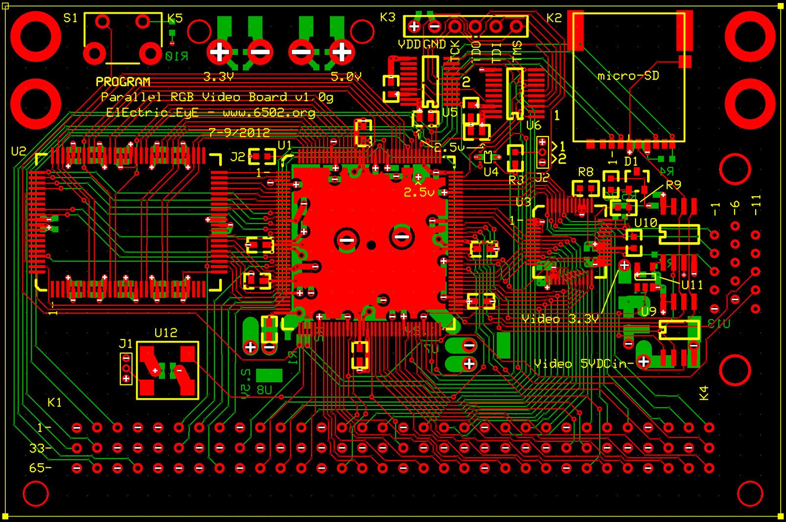
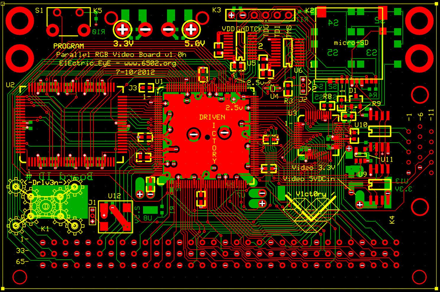
For v1.0h I've decided to add 4 pushbuttons which will fit on the backside of the MicroSD adapter. They will all be pulled high by a 4.7K resistor, when any of them are pushed. I will edit the constraint file to show the switch signals.
Re: Concept & Design of Parallel 16-bit VGA Boards
Posted: Mon Oct 08, 2012 1:28 pm
by Arlet
If you have some space, I'd also recommend adding a few test points,
like these, with a resistor + LED attached to each test point. That way you can provide a simple debug/status indicator through the LEDs, and attach a scope probe at the same time.
Re: Concept & Design of Parallel 16-bit VGA Boards
Posted: Tue Oct 09, 2012 12:27 am
by ElEctric_EyE
If you have some space, I'd also recommend adding a few test points...
I have avoided LEDs in this project, and anything else that may add inductance or any other possibility of noise. This v1.0g design takes successive hi-speed signals from previous boards, potentially at 108MHz. What' I've been doing for pin testing, is to cut about 4" length of .015" diameter WireWrap wire and wrap it around the scope probe and then test desired pins. Clearance is tight and requires a steady hand, but this works.
Now, if this were a BGA design, I can see how bringing out some pins as you've suggested, may help in troubleshooting...
EDIT: Corrected top MHz.
Re: Concept & Design of Parallel 16-bit VGA Boards
Posted: Tue Oct 09, 2012 5:58 am
by Arlet
You don't have any low speed signals that you can hijack for this purpose ? Something going to serial flash, or something like that.
Re: Concept & Design of Parallel 16-bit VGA Boards
Posted: Tue Oct 09, 2012 2:25 pm
by ElEctric_EyE
Why would you want to do this? or maybe which signals would you want to look at in particular? I could surely put in some holes to accomodate the test points, however there are only 3 holes left in v1.0h design.
Re: Concept & Design of Parallel 16-bit VGA Boards
Posted: Tue Oct 09, 2012 2:37 pm
by Arlet
Why would you want to do this? or maybe which signals would you want to look at in particular? I could surely put in some holes to accomodate the test points, however there are only 3 holes left in v1.0h design.
To make it easier to put a scope probe on a signal, and keeping your hands free at the same time. Holding a probe stable on a 0.5 mm pitch pin while fiddling with the knobs, or a second probe isn't very easy. The exact signals depends on thing I'd like to look at. The advantage of the FPGA is that you can bring out any signal (even a duplicate of an existing one) to any of the pins. For instance, if there's a weird problem that only happens once per second, you can try to create a trigger expression, and bring out that trigger signal to a test pin so you can capture it on the scope while probing any of the other signals at the same time.
Re: Concept & Design of Parallel 16-bit VGA Boards
Posted: Tue Oct 09, 2012 2:46 pm
by ElEctric_EyE
Why would you want to do this? or maybe which signals would you want to look at in particular? I could surely put in some holes to accomodate the test points, however there are only 3 holes left in v1.0h design.
To make it easier to put a scope probe on a signal, and keeping your hands free at the same time. Holding a probe stable on a 0.5 mm pitch pin while fiddling with the knobs, or a second probe isn't very easy...
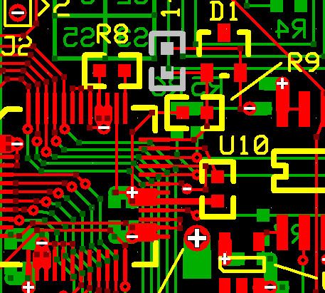
Ah, to let you in on a secret, all of the smallest (.008" I.D./.026" O.D.) vias on the board can snugly fit a stripped .010" WW wire into them even without soldering. While they are not guaranteed to be free of solder, looking at all 3 boards, not one of the vias is filled in.
A
CLOSEUP shows you the possibilities. v1.0h is virtually identical...
Re: Concept & Design of Parallel 16-bit VGA Boards
Posted: Wed Oct 10, 2012 3:37 pm
by ElEctric_EyE
A
CLOSEUP shows you the possibilities.
v1.0h is virtually identical...
Got some neato graphic designs on there too, heh. Will put the order in tomorrow.
Re: Concept & Design of Parallel 16-bit VGA Boards
Posted: Wed Oct 10, 2012 8:15 pm
by ElEctric_EyE
I hate that feeling right after I put in the order, and I realize I forgot to do 'such and such'. Well, I don't have that feeling this time around. I will order in 1 hr if I can't make another correction or add anything else. So what if it's potato soup for a week or 2!

Re: Concept & Design of Parallel 16-bit VGA Boards
Posted: Wed Oct 10, 2012 11:19 pm
by ElEctric_EyE
Order placed. ETA 3 days.
Used to be 3 days, now it's 5. Email says ETA is 10/18...
Re: Concept & Design of Parallel 16-bit VGA Boards
Posted: Wed Oct 17, 2012 6:21 pm
by ElEctric_EyE
Received the v1.0h boards today, 1 day ahead of schedule from ExpressPCB!
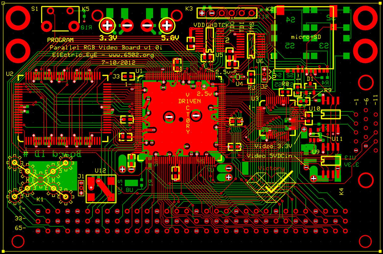
Already I have a
v1.0i in the works, although changes are purely cosmetic to the graphics at this point. Version 'i' should be the last, I think. I expect Arlet maybe will have some comments for possible improvements to add for the next PVB board run. We shall see his soldering skills!

Re: Concept & Design of Parallel 16-bit VGA Boards
Posted: Wed Oct 17, 2012 6:58 pm
by Arlet
Received the v1.0h boards today, 1 day ahead of schedule from ExpressPCB!
Already I have a
v1.0i in the works, although changes are purely cosmetic to the graphics at this point. Version 'i' should be the last, I think. I expect Arlet maybe will have some comments for possible improvements to add for the next PVB board run. We shall see his soldering skills!
Do you have schematics, by the way ?
Re: Concept & Design of Parallel 16-bit VGA Boards
Posted: Wed Oct 17, 2012 7:11 pm
by ElEctric_EyE
...Do you have schematics, by the way ?
No schematics, I find them to be a hamper. I rely solely on the board layout from the beginning of the design. This way there is no possibility of translation errors from schematic to board layout (also I didn't have room for labelling cap's on the board since they're so close together). The layout IS the schematic. I have made an effort to label resistors as they are usually unique values.... Thinking, there are some unique capacitors near the videoDAC. I will post an update for construction.
Re: Concept & Design of Parallel 16-bit VGA Boards
Posted: Wed Oct 17, 2012 7:23 pm
by Arlet
No schematics, I find them to be a hamper. I rely solely on the board layout from the beginning of the design.
I guess that works well when you can highlight traces on the screen and see the pin numbers, but I find it quite strenuous to try to follow the red/green lines through all the vias on the JPG, and count the pin numbers of the TQFP-100. Luckily, most of the important stuff is documented by the UCF file.
Re: Concept & Design of Parallel 16-bit VGA Boards
Posted: Wed Oct 17, 2012 8:40 pm
by ElEctric_EyE
..Luckily, most of the important stuff is documented by the UCF file.
Yes, the .UCF file is key, also the parts list. I've taken pains to keep everything updated. Schematics are a pain nowadays and would slow my progress.
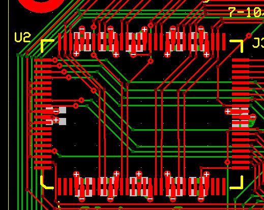
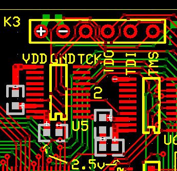
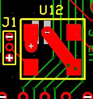
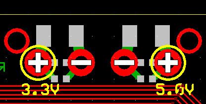
Some tips, in no particular order (parts are highlighted in white):
In regards to the:
(U2) SyncRAM: 2 0603 bypass cap's fit on each power pin on the bottom of the board.
(U5 & U6) FPGA PROMs: 4 0603 bypass cap's on the top.
(U12) 100MHz Oscillator: 2 0603 cap's on the bottom.
(3.3V & 5.0V mains): 2 1210 cap's, 4 0603 cap's on the bottom.
(U1): 7 0603 bypass cap's on top.
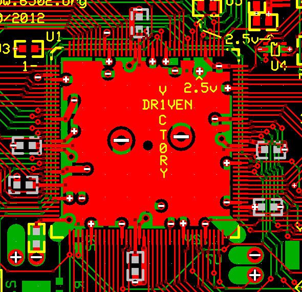
(U1): 14 0603 bypass cap's on bottom. 2 1210 bypass cap's on bottom center.
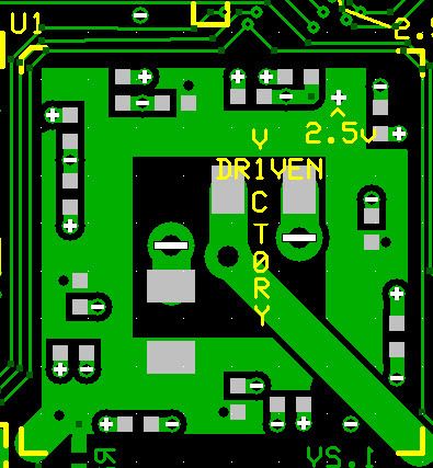
(U3): 1 0603 .1uF
(U3): 1 0603 1uF
Now in retro, would've been easier for schematics, sorry.

Pics are from v.0i, but everything is the same here. My mistake.