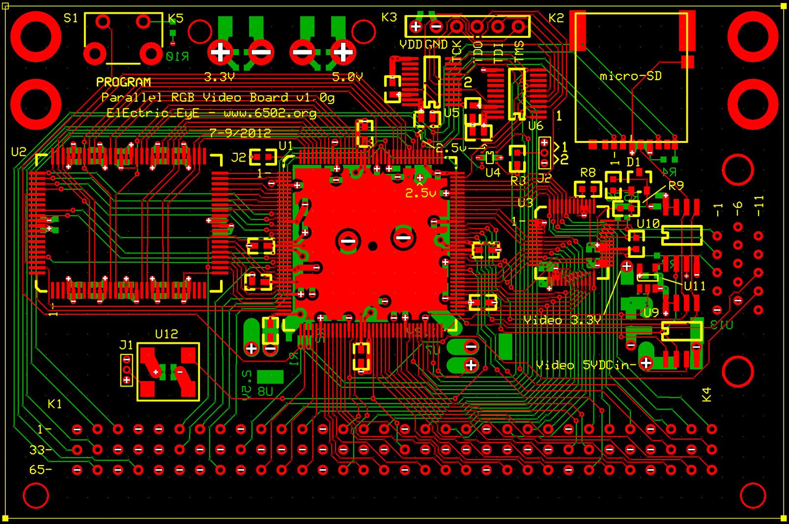
Concept & Design of 3.3V Parallel 16-bit VGA Boards
-
ElEctric_EyE
- Posts: 3260
- Joined: 02 Mar 2009
- Location: OH, USA
Re: Concept & Design of Parallel 16-bit VGA Boards
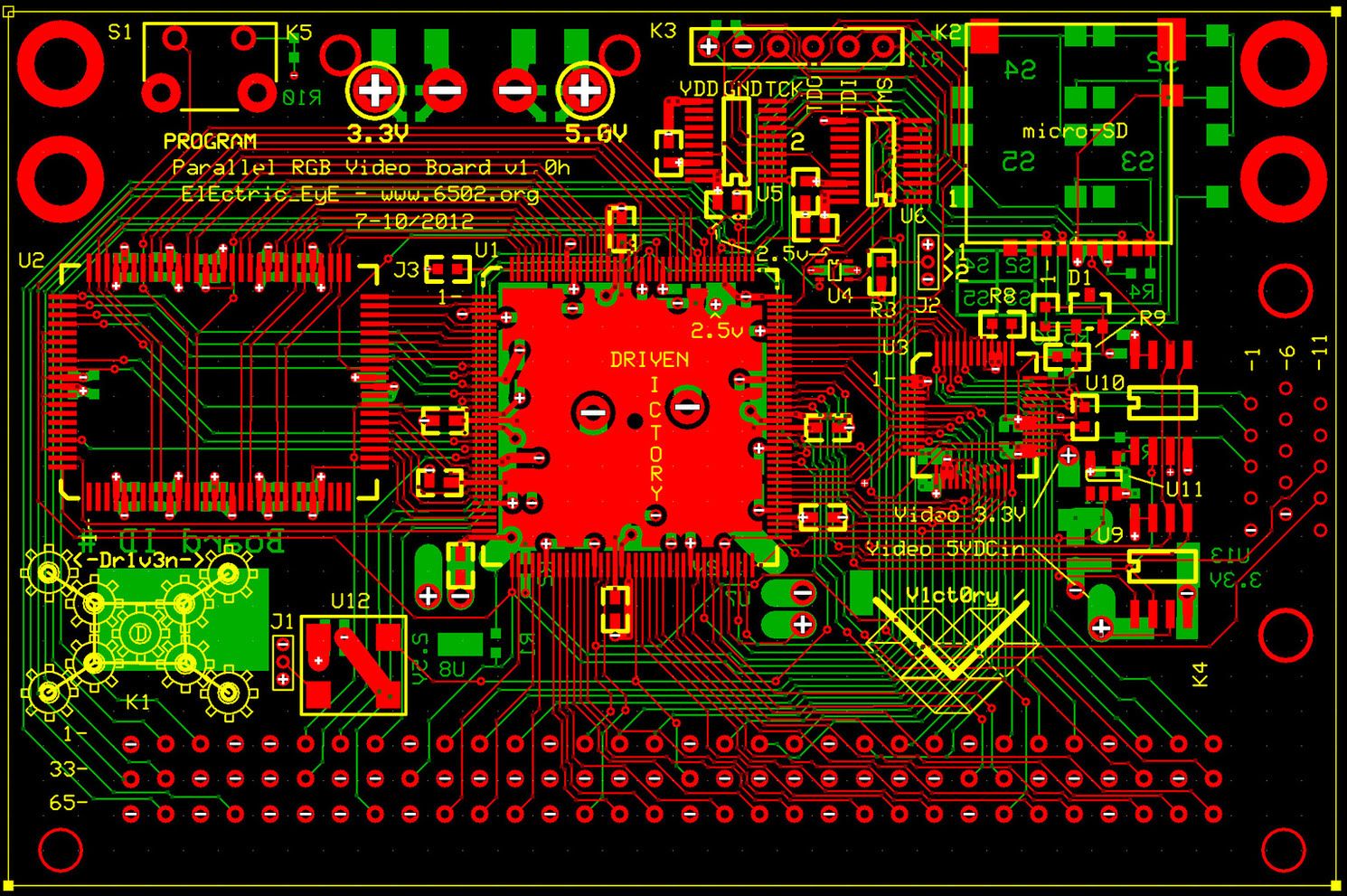
For v1.0h I've decided to add 4 pushbuttons which will fit on the backside of the MicroSD adapter. They will all be pulled high by a 4.7K resistor, when any of them are pushed. I will edit the constraint file to show the switch signals.

Re: Concept & Design of Parallel 16-bit VGA Boards
If you have some space, I'd also recommend adding a few test points, like these, with a resistor + LED attached to each test point. That way you can provide a simple debug/status indicator through the LEDs, and attach a scope probe at the same time.
-
ElEctric_EyE
- Posts: 3260
- Joined: 02 Mar 2009
- Location: OH, USA
Re: Concept & Design of Parallel 16-bit VGA Boards
Arlet wrote:
If you have some space, I'd also recommend adding a few test points...
Now, if this were a BGA design, I can see how bringing out some pins as you've suggested, may help in troubleshooting...
EDIT: Corrected top MHz.
Last edited by ElEctric_EyE on Tue Oct 09, 2012 10:46 am, edited 1 time in total.
Re: Concept & Design of Parallel 16-bit VGA Boards
You don't have any low speed signals that you can hijack for this purpose ? Something going to serial flash, or something like that.
-
ElEctric_EyE
- Posts: 3260
- Joined: 02 Mar 2009
- Location: OH, USA
Re: Concept & Design of Parallel 16-bit VGA Boards
Why would you want to do this? or maybe which signals would you want to look at in particular? I could surely put in some holes to accomodate the test points, however there are only 3 holes left in v1.0h design.
Re: Concept & Design of Parallel 16-bit VGA Boards
ElEctric_EyE wrote:
Why would you want to do this? or maybe which signals would you want to look at in particular? I could surely put in some holes to accomodate the test points, however there are only 3 holes left in v1.0h design.
-
ElEctric_EyE
- Posts: 3260
- Joined: 02 Mar 2009
- Location: OH, USA
Re: Concept & Design of Parallel 16-bit VGA Boards
Arlet wrote:
ElEctric_EyE wrote:
Why would you want to do this? or maybe which signals would you want to look at in particular? I could surely put in some holes to accomodate the test points, however there are only 3 holes left in v1.0h design.
A CLOSEUP shows you the possibilities. v1.0h is virtually identical...
-
ElEctric_EyE
- Posts: 3260
- Joined: 02 Mar 2009
- Location: OH, USA
Re: Concept & Design of Parallel 16-bit VGA Boards
Got some neato graphic designs on there too, heh. Will put the order in tomorrow.
-
ElEctric_EyE
- Posts: 3260
- Joined: 02 Mar 2009
- Location: OH, USA
Re: Concept & Design of Parallel 16-bit VGA Boards
I hate that feeling right after I put in the order, and I realize I forgot to do 'such and such'. Well, I don't have that feeling this time around. I will order in 1 hr if I can't make another correction or add anything else. So what if it's potato soup for a week or 2! 
-
ElEctric_EyE
- Posts: 3260
- Joined: 02 Mar 2009
- Location: OH, USA
Re: Concept & Design of Parallel 16-bit VGA Boards
Order placed. ETA 3 days.
Used to be 3 days, now it's 5. Email says ETA is 10/18...
Used to be 3 days, now it's 5. Email says ETA is 10/18...
-
ElEctric_EyE
- Posts: 3260
- Joined: 02 Mar 2009
- Location: OH, USA
Re: Concept & Design of Parallel 16-bit VGA Boards
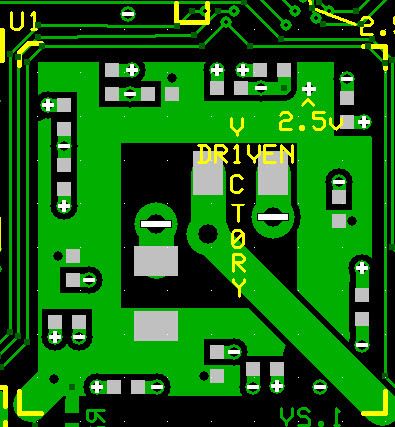
Received the v1.0h boards today, 1 day ahead of schedule from ExpressPCB!
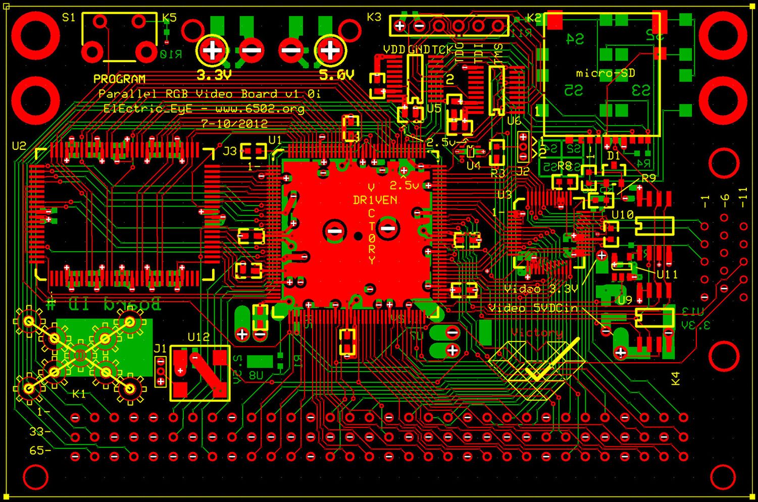
Already I have a v1.0i in the works, although changes are purely cosmetic to the graphics at this point. Version 'i' should be the last, I think. I expect Arlet maybe will have some comments for possible improvements to add for the next PVB board run. We shall see his soldering skills!
Already I have a v1.0i in the works, although changes are purely cosmetic to the graphics at this point. Version 'i' should be the last, I think. I expect Arlet maybe will have some comments for possible improvements to add for the next PVB board run. We shall see his soldering skills!
Re: Concept & Design of Parallel 16-bit VGA Boards
ElEctric_EyE wrote:
Received the v1.0h boards today, 1 day ahead of schedule from ExpressPCB!
Already I have a v1.0i in the works, although changes are purely cosmetic to the graphics at this point. Version 'i' should be the last, I think. I expect Arlet maybe will have some comments for possible improvements to add for the next PVB board run. We shall see his soldering skills!
Already I have a v1.0i in the works, although changes are purely cosmetic to the graphics at this point. Version 'i' should be the last, I think. I expect Arlet maybe will have some comments for possible improvements to add for the next PVB board run. We shall see his soldering skills!
-
ElEctric_EyE
- Posts: 3260
- Joined: 02 Mar 2009
- Location: OH, USA
Re: Concept & Design of Parallel 16-bit VGA Boards
Arlet wrote:
...Do you have schematics, by the way ?
Re: Concept & Design of Parallel 16-bit VGA Boards
ElEctric_EyE wrote:
No schematics, I find them to be a hamper. I rely solely on the board layout from the beginning of the design.
-
ElEctric_EyE
- Posts: 3260
- Joined: 02 Mar 2009
- Location: OH, USA
Re: Concept & Design of Parallel 16-bit VGA Boards
Arlet wrote:
..Luckily, most of the important stuff is documented by the UCF file.
Some tips, in no particular order (parts are highlighted in white):
In regards to the:
(U2) SyncRAM: 2 0603 bypass cap's fit on each power pin on the bottom of the board.
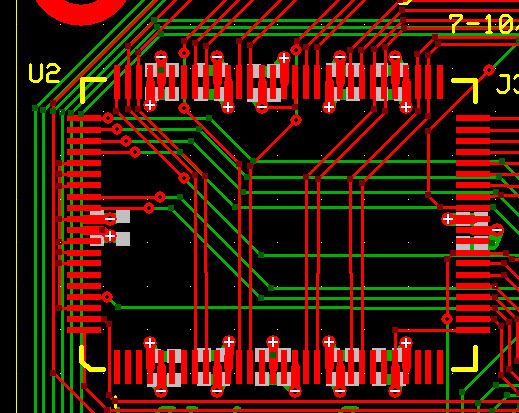
(U5 & U6) FPGA PROMs: 4 0603 bypass cap's on the top.
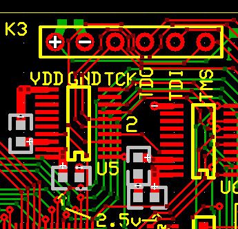
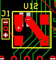
(U12) 100MHz Oscillator: 2 0603 cap's on the bottom.
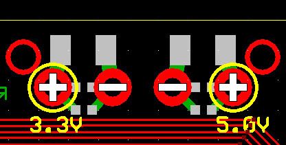
(3.3V & 5.0V mains): 2 1210 cap's, 4 0603 cap's on the bottom.
(U1): 7 0603 bypass cap's on top.
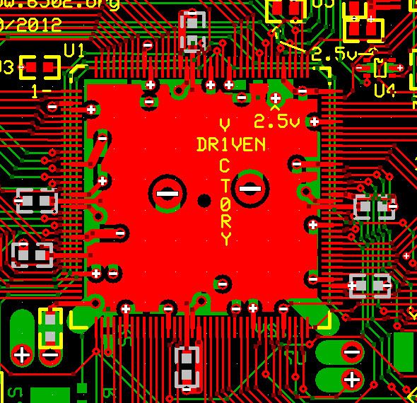
(U1): 14 0603 bypass cap's on bottom. 2 1210 bypass cap's on bottom center.
(U3): 1 0603 .1uF
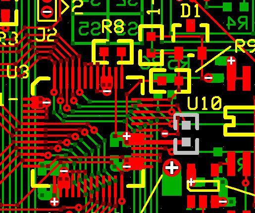
(U3): 1 0603 1uF
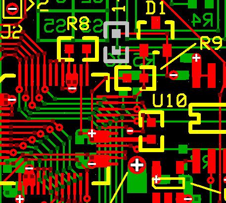
Now in retro, would've been easier for schematics, sorry.
Pics are from v.0i, but everything is the same here. My mistake.