Page 4 of 10
Re: Attempting to build a simple 6502 SBC from scratch
Posted: Sat Feb 25, 2023 4:38 am
by GARTHWILSON
I notice the headers attaching to VIA Port A and Port B are only 10 pins each. I'd suggest 14 or even 16 pins each so you can connect a ribbon cable to an external device and supply the device with power, ground and perhaps even an extra signal or two.
Re: Attempting to build a simple 6502 SBC from scratch
Posted: Sat Feb 25, 2023 6:47 am
by barnacle
They don't come in 8, 12, 18, etc. positions.
You can find them if you search for them:
https://www.lcsc.com/products/IDC-Conne ... c%20header but I would agree that ten pin (2x5) are handier to fit on ribbon cable

There is also the possibility of 0.05" (1.27mm) spacing IDC headers and connectors to reduce board space, but adaptors between the two are clunky.
Neil
Re: Attempting to build a simple 6502 SBC from scratch
Posted: Sat Feb 25, 2023 7:34 am
by GARTHWILSON
Well, that's new to me. I haven't been watching for new sizes, but I'm sure those others didn't exist 20 years ago. Regardless, for best availability, it's probably best to stick to the number of positions I mentioned. IDCs are specifically the ones that go on the cable, like this:
Here's one not yet mounted, let alone with the strain reliever attached:
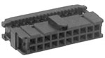
- IDC20.jpg (4.61 KiB) Viewed 172227 times
These plug onto the male pin headers on the board.
Re: Attempting to build a simple 6502 SBC from scratch
Posted: Sat Feb 25, 2023 9:24 am
by Michael
Skinny (0.3") 64K SRAM chips are available at a nice price and take up less board space. I've been very happy with the
SRAM chips from this vendor;
Re: Attempting to build a simple 6502 SBC from scratch
Posted: Sat Feb 25, 2023 11:11 am
by and3rson
I notice the headers attaching to VIA Port A and Port B are only 10 pins each. I'd suggest 14 or even 16 pins each so you can connect a ribbon cable to an external device and supply the device with power, ground and perhaps even an extra signal or two.
[...]
Alternatively, the oscillator could be relocated. Right now the width of the board (from west to east) is consumed by...
- oscillator, CPU, RAM, ROM, VIA. Instead, you could try...
- ROM, RAM, CPU, VIA
The ROM (in its ZIF socket) is comparatively bulky, which is one reason I think it might do well at the edge of the board. Half of that extra width can hang over the edge! Oh, and I was thinking the CPU would be oriented with pin 1 toward the north, whereas the RAM, ROM and VIA would have pin 1 toward the south. This will tend to untangle some of the bus lines, but maybe with the auto-router you won't worry about that. Still, it'd be interesting to see what it would produce if you start by arranging the chips as I suggest.
Whether you do or don't reorient the chips, I would still consider moving the oscillator. With the extra width that's freed up, maybe those two headers for Port A and Port B could snuggle up broadside right next to the VIA instead of being pushed off the end. Just an idea... Good luck with the project, and have fun!
Well, what do ya know - that worked like a charm!
I've already had CPU & VIA turned 180 degrees - that drastically minimized the amount of rat nests. However moving the ZIF socket to the edge actually freed up a LOT of space - I guess I could have crammed an entire ACIA or SID in there!
The new layout is much more optimal, albeit a bit more scattered. In my previous version, I really liked how the power & clock section nicely occupied the leftmost column, and I also liked how chips followed the same order as in schematic, but hey - getting some extra clearance for I/O is more important than that!

Here's my new design. Everything is gravitated a bit too much to the left since I was trying to utilize as much space as I could. I'll increase spacing between the components once I'm satisfied with the overall layout.
Michael - I wish I knew about it in the beginning!

I've already ordered full-width DIP-28 SRAMs, so I guess I'll stick to them for the time being. Still gonna order a bunch of those since they are really cheap!
Garth - thank you for all the tips on ribbon clearance. I've updated my pinout so that it is reverse-tolerant, and also added power rails to each VIA port - that makes a lot of sense.
Dr Jekyll - apologies for the color image of the PCB, it totally flew over my head. No more vividly colored schematics from me!
EDIT: Darn, I forgot to bump the version number to 0.8 on the silkscreen.
EDIT 2: Totally forgot - in case someone's interested, all my stuff is open-source, you can find all schematics & sources here:
https://github.com/and3rson/m6502
EDIT 3: I've moved my I/O from $C000-$CFFF to $D000-$DFFF so that in future I can put SID on $D4xx for compatibility with C64.
Re: Attempting to build a simple 6502 SBC from scratch
Posted: Sat Feb 25, 2023 1:24 pm
by plasmo
Cool, now you have room to add a 40-pin RC6502 connector for video/keyboard and multi-channel serial boards. Then again, maybe that's too aggressive for first board.
Bill
Re: Attempting to build a simple 6502 SBC from scratch
Posted: Sat Feb 25, 2023 2:10 pm
by Dr Jefyll
that drastically minimized the amount of rat nests.
Okay, cool! But what you've done doesn't quite match what I had in mind. And it might be possible to reduce the rats nests even further.
I couldn't spin the ZIF socket around because then the release arm would be hard to reach. But I do want the
chip spun around, and of course that's easily done. In other words I'm suggesting you ignore the Pin 1 marking on the ZIF socket and always insert the ROM "backwards" -- ie, with Pin 1 toward the south. (You do have the somewhat goofy option of obscuring the original marking on the socket and making your own label to indicate where pin 1 belongs!


)
If the chips are spun as shown (ie, CPU with pin 1 toward the north, and RAM, ROM and VIA with pin 1 toward the south) then I suspect the traces will become even tidier, and probably have fewer vias. I could be wrong, but it might be worth a try. BTW, notice how the four main chips are aligned to one another in terms of north-south; this too is part of the plan, and probably shouldn't be changed much.
One final suggestion (for now, at least)! You could save some more space by using a SIP resistor array to replace all the individual pullup resistors.
-- Jeff
Re: Attempting to build a simple 6502 SBC from scratch
Posted: Sat Feb 25, 2023 2:17 pm
by barnacle
That circuit board appeals much more to my sense of tidiness; I feel that automatic layout sometimes doesn't have the same aesthetic that I do
But then, I enjoy laying out a board with lots of chips... here's my 6502 SBC, which is easy, and a slightly more complex 8080 discrete component ALU.
Neil
Re: Attempting to build a simple 6502 SBC from scratch
Posted: Sat Feb 25, 2023 2:23 pm
by barnacle
@Jeff - I learned a long time ago that not having all the chips on the board facing the same way is a potential recipe for disaster. Sooner or later I'm bound to stick one in upside down!
If only the designers of 1970's processor packages had looked into the future and seen big JEDEC pinout memories and made their processor pinouts match

Neil
p.s. Am I the only one around here who uses SM passives mixed with PTH parts?
Re: Attempting to build a simple 6502 SBC from scratch
Posted: Sat Feb 25, 2023 2:33 pm
by Dr Jefyll
I do agree that there's a tradeoff involved, Neil. Sometimes (and perhaps quite commonly) a more compact design will come at the cost of decreased convenience in regard to remembering where pin 1 is found. One is obliged to weigh one priority against another, but that's nothing new... in fact it's the essence of engineering! And the "right" choice for one situation won't necessarily match the right choice where different circumstances and priorities prevail.
I suppose we should be grateful, not annoyed, at this complexity. Think how boring life would otherwise be!

ps: Good point, and thanks for the reminder. And no you're not the only one. Mixing SM passives into a through-hole design is a great idea. And those pullups I mentioned would be good candidates for replacement with SMT.
-- Jeff
Re: Attempting to build a simple 6502 SBC from scratch
Posted: Sat Feb 25, 2023 4:33 pm
by and3rson
@Jeff - that's a good idea! But knowing my short memory, I think I'll keep it as it is now since there's very little rat nests now.
@Neil - yeah, rotated 6502 & VIA were the only ways for me to go. I wish pin ordering matches the modern one, but hey, as they say - "One does not ask God for supplements.".
Also, after giving it more thought, I've decided to expose Ф2, R/W, /RD, /WD, /RES, /IRQ, data & address buses, and more power rails via pin headers. This will allow me to play with SID & ACIA later using a separate daughterboard or even a breadboard.
Here's what it looks line now.
EDIT: Forgot to rotate J4 & J6 to reduce the rat nest in there, and also to have them oriented the same way as other 4 headers.
EDIT 2: Seems like newer versions of phpbb support overline via
syntax, which is simply translated into
Code: Select all
<span style="text-decoration: overline">TEXT</span>
. This should be easy to add, I've checked 6502org on Github hoping to find a repo for this forum's phpbb installation in order to create a pull request, but seems like it's not there.
Re: Attempting to build a simple 6502 SBC from scratch
Posted: Sat Feb 25, 2023 4:45 pm
by Paganini
If you don't mind ponying up a little extra for an Aries ZIF socket (about $11 on Digikey, IIRC), you can face it however you want without worrying about the release arm.
This is turning into a great looking board, BTW! I might want one.
Re: Attempting to build a simple 6502 SBC from scratch
Posted: Sat Feb 25, 2023 4:48 pm
by and3rson
If you don't mind ponying up a little extra for an Aries ZIF socket (about $11 on Digikey, IIRC), you can face it however you want without worrying about the release arm.
This is turning into a great looking board, BTW! I might want one.
Thanks! I'm flattered.
Aries are super-nice, especially the low-profile ones... But man, are those expensive!
Re: Attempting to build a simple 6502 SBC from scratch
Posted: Sat Feb 25, 2023 5:57 pm
by BigDumbDinosaur
If you don't mind ponying up a little extra for an Aries ZIF socket (about $11 on Digikey, IIRC), you can face it however you want without worrying about the release arm.
That was something I mentioned a few posts back. The socket is only a tad bigger than the chip that fits in it.
Re: Attempting to build a simple 6502 SBC from scratch
Posted: Sat Feb 25, 2023 6:17 pm
by GARTHWILSON
It's looking really nice. Remember that if it helps get things routed, you can mix up the data lines to SRAM, and mix up the address lines to it too. You can do this for ROM as well, but if you do, you'll need to make a programming adapter, whether in hardware or in software, to pre-scramble things so that they come out right on the board with its connections. (This is the first tip in my "Tip of the Day" column I ran 22 years ago, at viewtopic.php?f=7&t=342 . Most if not all of these tips are repeated somewhere in the 6502 primer, just not all together.)
As for the ZIF socket, I've had better luck with the smaller Aries one that BDD and Paganini have recommended above, than with the 3M one. The latter seems to suffer more from intermittent connections.