Page 4 of 4
Re: CPLD Driven color VGA
Posted: Wed Aug 29, 2018 2:36 pm
by cbmeeks
I'm curious on the oscillator. I see that you're going to use a 25.175 MHz oscillator. Which is the standard VGA spec. Now, I'm pretty new to PLD's in general but I thought you needed to use a higher frequency so that it can be divided down?
For example, I've seen people use a 2 MHz oscillator through a flip-flop in order to get 1 MHz. Do CPLD's not need that? In other words, can a 25.175 MHz oscillator on one of the GCLK pins still operate at the full 25.175 MHz?
Thanks.
Re: CPLD Driven color VGA
Posted: Wed Aug 29, 2018 11:04 pm
by MichaelM
Most modern oscillators are specifically designed to produce 50% duty cycle signals within a percent or two. That is generally good enough for most circuits, including PLDs. To the best of my understanding, dividing a clock source by 2 (or 4) is primarily done to ensure that the resulting clock signal also has a 50% duty cycle.
In the past I've had some trouble constructing oscillators in the 1MHz range, so I would use a higher frequency crystal and divide it down as needed by the circuits I was supplying with the clock.
Re: CPLD Driven color VGA
Posted: Thu Aug 30, 2018 12:23 am
by LIV2
First I'll preface by pointing out I have no idea what I'm doing

My limited understanding of putting the oscillator behind a flip-flop is that it does the following:
* Guarantees a 50% Duty Cycle
* Cleaner/quicker rise and fall
* More drive current meaning it can handle more load
I looked at the spec sheet for the oscillator and it can drive 15ma vs a 74HC574's 35ma.
In my case I'm only driving 3 inputs and if seems to work fine, the oscillator is specced for a 50% duty cycle so it all seems fine so far.
My main clock is also driven directly by a can oscillator but that's because I was naive when I designed the board. When I do my next main board it'll use a flip-flop
Re: CPLD Driven color VGA
Posted: Thu Aug 30, 2018 1:22 am
by MichaelM
A FF divider is always an option but not always necessary to provide a 50% duty cycle with increased drive levels. A properly chosen buffer may be all that's necessary. Look for a logic family, like many of the CMOS logic families, where the output drive levels are symmetric. If the loads are balanced, then I expect the balanced drive levels will preserve the duty cycle of the oscillator.
Re: CPLD Driven color VGA
Posted: Thu Aug 30, 2018 12:13 pm
by cbmeeks
That makes sense. Thanks for the clarification both of you.
Re: CPLD Driven color VGA
Posted: Wed Oct 24, 2018 1:13 am
by LIV2
Got some PCBs made, ordered via JLCPCB and am pretty happy with the results!
There are some jumpers to change the address decoding in case I decide on changing my memory map
I also added a jumper that allows you to tie /OE high on the memory port used for the host memory access. This way the VRAM can overlay system ram without having to drive another signal to the glue logic inhibiting the on-board ram.
Thanks everyone for your help making this happen!
Re: CPLD Driven color VGA
Posted: Wed Oct 24, 2018 1:42 am
by Dr Jefyll
I also added a jumper that allows you to tie /OE high on the memory port used for the host memory access. This way the VRAM can overlay system ram without having to drive another signal to the glue logic inhibiting the on-board ram.
Good idea. BTW, what sort of system does this board plug into? Sometime it'd be nice to hear about that project.

Thanks everyone for your help making this happen!
Glad we could help. You've done a very tidy job -- it turned out great!
-- Jeff
Re: CPLD Driven color VGA
Posted: Wed Oct 24, 2018 3:28 am
by LIV2
I should do a proper writeup on the system for sure. There's some documentation in my github here (schematics, images)
https://github.com/LIV2/Homebrew-65C02-Computer
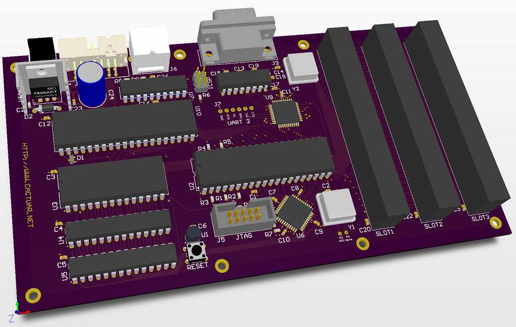
Basically it consists of
* 4-layer PCB
* WDC 65C02 currently running at 10MHz
* SC28L92 DUART
* PS/2 Keyboard port
* Glue logic driven by an Altera EPM7064S CPLD
The layout is pretty terrible (which is why I haven't really shown it off), because of the way I laid out all the ICs the traces are very long (I naively did that thinking it was better than having a boatload of vias)
The 28L92 placement might seem odd but that's because I originally laid everything out with a 65C51