Page 4 of 6
Re: Future plans for Dev. Board v1.2
Posted: Mon Jul 16, 2012 11:58 pm
by ElEctric_EyE
I've found a smaller IC of the same Analog Devices 7511 family, the 64-pin QFP
ADV7511W. Some very impressive spec's (8-channel audio!), I think I can make it work. There should be 1 more 38-pin TSSOP
IC to protect the front end of this IC for hot plug operation.
When I complete the board layout, I'll make a new thread. Should be within 2 days time.
Re: Future plans for Dev. Board v1.2
Posted: Tue Jul 17, 2012 4:36 am
by BigDumbDinosaur
I've found a smaller IC of the same Analog Devices 7511 family, the 64-pin QFP
ADV7511W.
And it's five volt tolerant too!
Re: Future plans for Dev. Board v1.2
Posted: Tue Jul 17, 2012 11:04 am
by ElEctric_EyE
Got the parts in. For sure Cypress deserves mention because I had to buy the SRAM direct from their online store as noone else had any in stock. I just paid for the IC's (I got 2 @$38ea) and shipping was free. Overnight shipping! So great job there. Not sure about shipping overseas though...
So quickly placing the DB15 VGA connector in the upper left and the SDcard adapter in the upper right of a spare 3.8"x2.5" devboard, there's just enough room for the JTAG connector in the middle. The mini HDMI connector will have to be mounted on one of the sides. HDMI IC's
will be made to fit somehow!
The force needed for the push-in/push-out action of the SDcard adapter seems abit much, but hopefully it will break in over time. The holes I place will have to be a perfect match for the mounting tabs, so as not to encourage any movement when pressing down. This is why I brought my digital micrometer home from work, just to double check the spec sheets. Also, the fit of the 96-pin main female connector to it's receptacle has a good feel, almost like a snap when it's fully seated. Not too difficult to pry apart either despite the large number of pins. I imagine it will be even easier with a board connected to it, where one can grasp the board to unseat it.
Anyway, back to work (play).

Re: Future plans for Dev. Board v1.2
Posted: Wed Jul 18, 2012 2:06 pm
by ElEctric_EyE
For RGB-in I need 24 pins. Does anyone foresee a problem if I use 22 pins from one IOB and the other 2 pins from another IOB?
EDIT: Arg! I don't have enough pins for 24 bit video. Gonna have to go with 16-bit, 5-6-5 RGB. This will free up quite a few pins, but I'm going to have to rearrange some things. Won't meet my deadline though.
Re: Future plans for Dev. Board v1.2
Posted: Wed Jul 18, 2012 4:54 pm
by BigEd
You're assuming that the fastest you can clock RGB between the boards is the same as the pixel clock rate you need, I think. Is that a valid assumption? If you can double-clock your RGB transfers, or otherwise multiplex the data, you don't need so many pins.
Re: Future plans for Dev. Board v1.2
Posted: Wed Jul 18, 2012 6:17 pm
by ElEctric_EyE
You're assuming that the fastest you can clock RGB between the boards is the same as the pixel clock rate you need, I think. Is that a valid assumption? If you can double-clock your RGB transfers, or otherwise multiplex the data, you don't need so many pins.
Well, this is a good thought but I think we might have to settle with 565. For this board, and the concept of having multiple boards working on the same image I would like for the resolution to be as high as possible. This means high speed is needed. Multiplexing usually means a slowing down of things in a non-pipelined system. Plus, all clock signals coming off the FPGA already go through a DDR Flip-Flop.
Re: Future plans for Dev. Board v1.2
Posted: Wed Jul 18, 2012 6:24 pm
by ElEctric_EyE
Now let me ask Arlet something if I may:
Right now I have the FPGA in the middle of the data path between the SRAM and videoDAC. Currently this uses 16 pins for the data bus and 24-pins for the RGB data.
Could I hook the SRAM directly to the videoDAC and have the FPGA tap off of that 16-bit bus? and in addition provide 8 more signals to the DAC? This would potentially save 16 pins.
Re: Future plans for Dev. Board v1.2
Posted: Wed Jul 18, 2012 7:06 pm
by ElEctric_EyE
Well, thinking back to the old days of discrete components using a 6545 and 6502, a typical video system would be organized as I described above and be able to freely do R/W operations to the video RAM during non-display periods. I'm just not sure how tight timings are nowadays with LCD/TFT/PLASMA Hi-Def displays, i.e. if the non-display periods offer any appreciable time to modify video memory since we are not waiting for an old style CRT gun to do a retrace.
Re: Future plans for Dev. Board v1.2
Posted: Wed Jul 18, 2012 10:01 pm
by ElEctric_EyE
Bah! The FPGA will have to be the arbiter for videoRAM access in a parallel system, so it must be in the middle, thereby imposing it's own ~7.5ns delay. The bottleneck will be the total delay added after all anticipated boards to be hooked up are wired in. This seals in the 5-6-5 configuration.
Re: Future plans for Dev. Board v1.2
Posted: Thu Jul 19, 2012 3:36 am
by Arlet
Could I hook the SRAM directly to the videoDAC and have the FPGA tap off of that 16-bit bus? and in addition provide 8 more signals to the DAC? This would potentially save 16 pins.
No, that would be very inflexible.
The FPGA will have to be the arbiter for videoRAM access in a parallel system, so it must be in the middle, thereby imposing it's own ~7.5ns delay.
The video signal would just arrive a bit later, but as long as you also delay the hsync/vsync signals by the same amount, that wouldn't matter at all. In practice, you would just delay everything by a couple of clock cycles.
Re: Future plans for Dev. Board v1.2
Posted: Thu Jul 19, 2012 9:26 pm
by ElEctric_EyE
Ok, thanks for your guys' input.
I'm nearing completion as I've decided not to add HD to the board. There's no need to have it on every board, just the last one in the chain. Best to add it in as a future HDMI plug-in module. All I have left are the FLASH IC's and wire up the main connector.
So I am back to thinking of how to communicate with this video board. Hardware-wise I'm thinking of a 4-bit parallel with a high speed clock, halt and RW lines. 4 bits is good because it evenly divides into 16-bits for color and 12-bits for X and Y positional data. The halt and clock would come from the FPGA. The clock would be a hopeful 100MHz phase 2. There would be 3 modes that would use the internal high speed blockRAM differently.
Mode 1 would be plot pixel/color. 40 bits of write only information needed. Halt would stay active after the last bit is received and until the buffer counter is reset to zero. When halt is active, actual plotting is happening.
Mode 2 would be plot line, circle, box. ***sorting out details***
Mode 3 would be plot a datastream. First X and Y start coordinates are sent. Then a width value is sent. And finally a 24-bit file size value is sent. This would allow for 8M pixels. Halt is sent to reset the buffer counter. This buffer in the blockRAM hopefully will be >4Kx16. Halt is sent each time the buffer is full and plotting begins.
This is all controlled by software. I'm pretty sure I can handle this part. A hardware state machine would obviously be far superior though.
These are just my initial thoughts of what to do with 2 global clock pins and 5 general pins.
Re: Future plans for Dev. Board v1.2
Posted: Fri Jul 20, 2012 12:10 am
by ElEctric_EyE
Ok, so let's loose modes 2 & 3. I would've to had mode defining bits anyway. Pins I don't have.
So now we have just 1 mode assumed, always. 40 bits to define pixel location (X+Y=24bits) and it's color(16bits). Imagine if it were across 8 boards plotting in the delayed pipeline.
Now I need to remind myself for future development of the 65Org32 and it's potential in controlling a multiple of these graphic boards. Or even a very simple version of a 65Org64. This would ideally be just a special CPU doing a load/store/shift/and/or/xor, with one addressing mode, on the RGB bits.
EDIT. Will have to add a CS line to communications too.
Re: Future plans for Dev. Board v1.2
Posted: Fri Jul 20, 2012 10:39 pm
by ElEctric_EyE
Now that I am 99% done, of course an idea comes to mind which shatters all my work this past week on board layout. I am not confident in my mode of communications which leads me to keep thinking of alternatives that have potential. Although the Spartan 6 is great for embedded CPU and high speeds signals, I am not convinced I need a CPU so close to the video out signal, especially since the 144 pin package is lacking.
All I really need is to make Arlet's SDRAM SDRAM video interface work with the SRAM. What I mean is to put those 3 modules (4 minus SD interface) into a Xilinx Coolrunner IIXL QFP package style 208-pin CPLD. There is a 208-pin QFP version with clock doubling/dual edge FF tech, sounding similar to DDR of the S6 FPGA.
All the pins would include:
41pins = 22 address + 16 data + 3 clock. CLK, CS, WE for synchronous RAM.
19pins = 16 RGB in +3 clock. HSYNC in, VSYNC in, pixelclock in for previous video board input.
20pins = 16 RGB out + 4 clock. Blank out, pixelclock out, HSYNC out, VSYNC out for videoDAC.
41pins = 22 address + 16 data + 3 clock. CLK, CS, WE for synchronous RAM interface for external CPU.
5pins = SI, SO, SCK, 2 CE for 3 SPI FLASH and 1 SDCard
-------
126pins
With the CPLD, we would loose the ability to have multiple configs, which is ok. Gonna have to refresh my memory oof Xilinx CPLDs. Been with FPGA's too long.
Ah shoot! I just remembered Arlet's code uses blockRAM not present on CPLDs. Is there hope using a string of FF's to hold one horizontal line of video data in a CPLD?
***buries head in hands***
I need BGA Infrared lasers to mount BGA packages!
Re: Future plans for Dev. Board v1.2
Posted: Fri Jul 20, 2012 11:55 pm
by ElEctric_EyE
Now that I am 99% done...
I was almost done! The SDCard adapter was next to the last thing to be fitted along with the reconnects to the SPI FLASH. The connections to the VGA connector would have finished the layout. SDCard adapter was going to be tight, some of it sticking above the board...
Re: Future plans for Dev. Board v1.2
Posted: Mon Jul 23, 2012 12:16 am
by ElEctric_EyE
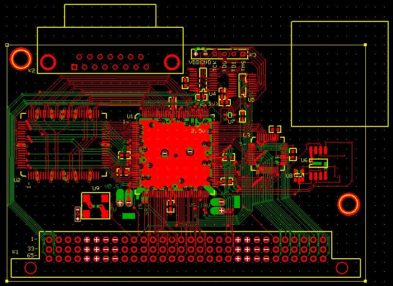
The 29mmx29mm SDcard connector will not fit. However, a 21mmx23mm miniSDcard connector will fit in the current board layout. I will order this part soon.
So I'll have 3 video boards...
Then I'll need to make the interconnecting base boards...
Then I'll need to make a controlling board that plugs into a base board that controls multiple VGA video boards with the overlying pixels/images.
So anyone can see the cost of a 3 individual board design is going to be abit costly @$100 3xeach , so I was/am still a little hesitant at the main video board design with very limited comm. In other words, I need committed volunteers.