Page 4 of 8
Posted: Fri May 07, 2004 5:23 am
by Ruud
Hallo Fabrice,
> the databus of the 6502 is always in input mode when PHI2 is (L).
> (IIRC, no datasheet to check it)
Please see:
http://www.funet.fi/pub/cbm/documents/c ... 50x-05.gif
http://www.funet.fi/pub/cbm/documents/c ... 50x-06.gif
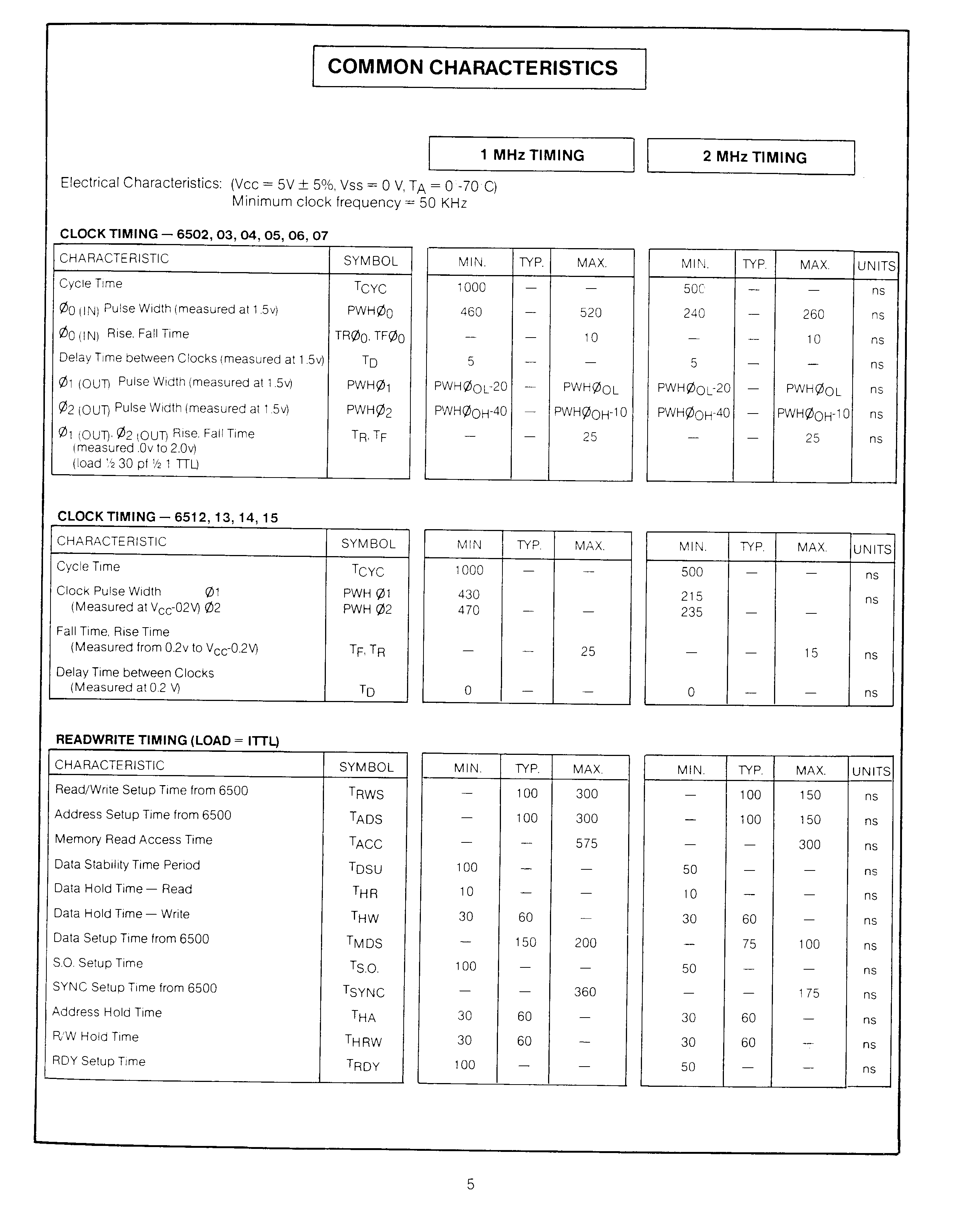
Trws is the setuptime for the R/W signal. It becomes active between 100-300 ns. after the falling edge of PHI2. I cannot imagine that the video display does his job within these 100 ns. Where can I find schematics of this 6502-system?
Posted: Fri May 07, 2004 5:50 am
by Ruud
Hallo Ruud,
> Trws is the setuptime for the R/W signal. It becomes active between
> 100-300 ns. after the falling edge of PHI2.
Stupid you! That the R/W is (L) does not mean that the 6502 start outputting data as well at the same time.
I just realised that when reading the thread about multi-processing: the old Commodore IEEE drives use two 650x processors, one running on the inversed clock of the other.
Posted: Fri May 07, 2004 8:28 am
by Euphoric
That the R/W is (L) does not mean that the 6502 start outputting data as well at the same time.
I just realised that when reading the thread about multi-processing: the old Commodore IEEE drives use two 650x processors, one running on the inversed clock of the other.
Yep, the data lines of the 6502 are in high-impedance mode during the low part of the clock, not in input mode. This feature has been used, as you mentionned, in multi-processor designs (using the 6512 brother I think. My memory is failing but I seem to remember there was a BBC system with two 65xx processor too), and in systems where the data bus is used by the video system during the low part of the clock (e.g. Microtan 65 does one video memory access during the low clock, and Oric systems even do two (using a 2/3-1/3 clock))...
Fabrice
Posted: Mon May 10, 2004 10:39 am
by Ruud
For those who forgot: the addresslines A16..23 of a 65816 are generated by latching the databus when PHI0 is (L). Some designs I encountered simply inverted PHI0 and used the resulting signal to clock a 74ALS574. The problem was that when RDY was activated, the latch started clocking the actual data, not the intended address. So I thought about a SCH to solve this problem.
The promised schematic:
Code: Select all
                                          \----\
PHI0  ------+------------------------------\    \
            |                               >    >O------+------------------- PHI1
RDY   ---+  |                      +-------/    /        |
         |  |                      |      /----/         |
         |  |                      |                     |     \----\
         |  |                      |                     +------\    \
         |  |                      |                     |       >    >O----- PHI2
         |  |                      |                     +------/    /
         |  |                      |                           /----/
         |  |                      |
         |  |                      +----------------------------------------+
         |  |                                                               |
         |  |                             |----)                            |
         |  +-----------------------------|     )              |----)       |
         |  |                             |      )O------------|     )      |
         |  |         \----\       +------|     )              |      )O----+
         |  |    +-----\    \      |      |----)         +-----|     )      |
         |--|----+      >    >O----+                     |     |----)       |
         |  |    +-----/    /                            |                  |
         |  |         /----/                             +-------\ /--------+
         |  |                                                     X
         |  |                                            +-------/ \--------+
         |  |                                            |                  |
         |  |                                            |     |----)       |
         |  |                             |----)         +-----|     )      |
         |  +-----------------------------|     )              |      )O----+
         |                                |      )O------------|     )
         +--------------------------------|     )              |----)
                                          |----)
Hmmmm, copy and paste it to a simple editor using a fixed font.
The base of the idea is that PHI0 for a 65816 can be hold (H) as long as you want to. My experiments prooved that at least the Acorn Atom need a delay between PHI0 and PHI2. In my original 6501/65816 convertor this job is done by two 04 invertorgates. The top NOR-gates take care of this funtion. The moment RDY becomes (L) and PHI0 is (H), a FlipFlop made out of two NAND-gates is set blocks the first top NOR-gate, causing PHI2 to remain (H) until RDY becomes (H) again when PHI0 is (H) as well.
Remarks:
- IMHO the RDY input of the 65816 is not needed anymore.
- the generated PHI2 may not be used for 6522's or other IC's that use PHI2 for their internal clocks.
Groetjes, Ruud
Posted: Mon May 10, 2004 4:00 pm
by Euphoric
Hello Daryl, here are a few opinions that were raised on the newsgroups:
- someone wondered if the PCB could be done with 2 layers only (even if this would need some patches), that would surely lower the price...
- as the module is very small, someone else proposed to group several modules on the same PCB. We would then saw the board to separate the duplicated modules...
Myself, I rather miss your previously proposed PCB, the one with the big DIP40 65816 and the surface mounted logic underneath it... Some of the people who declared interest for the module have already been part of Mike's CPU bulk order, so we already have some 65816 in DIP40 form, but not in QFP form (and as far as I am concerned, I have never soldered a QFP chip)... Could you remind me why you were not happy with your PCB that used a DIP40 65816 ?
Best regards,
Fabrice
Posted: Tue May 11, 2004 5:51 am
by Ruud
Hallo allemaal,
> The promised schematic:
Garth was so friendly to tell me that my SCH didn't look to well in the Forum: the SCH is not only shown with a variable font but all extra spaces are gone as well !!! So copy and paste would not work.
But now the very strange thing. As you can see I replied my own message and to my big suprise in the reply the SCH is still shown with a variable font but all spaces are there! I copy and pasted that in my editor et voilá, the SCH shows up as it should!
It seems I have to make a real SCH, turn it into GIF and place it on my site. I'll notice you.
Posted: Tue May 11, 2004 6:30 am
by dclxvi
Garth was so friendly to tell me that my SCH didn't look to well in the Forum: the SCH is not only shown with a variable font but all extra spaces are gone as well !!! So copy and paste would not work.
Just stick the schematic inside
code and
/code tags (with each tag surrounded by square brackets, of course), like so:
Code: Select all
                                          \----\
PHI0  ------+------------------------------\    \
            |                               >    >O------+------------------- PHI1
RDY   ---+  |                      +-------/    /        |
         |  |                      |      /----/         |
         |  |                      |                     |     \----\
         |  |                      |                     +------\    \
         |  |                      |                     |       >    >O----- PHI2
         |  |                      |                     +------/    /
         |  |                      |                           /----/
         |  |                      |
         |  |                      +----------------------------------------+
         |  |                                                               |
         |  |                             |----)                            |
         |  +-----------------------------|     )              |----)       |
         |  |                             |      )O------------|     )      |
         |  |         \----\       +------|     )              |      )O----+
         |  |    +-----\    \      |      |----)         +-----|     )      |
         |--|----+      >    >O----+                     |     |----)       |
         |  |    +-----/    /                            |                  |
         |  |         /----/                             +-------\ /--------+
         |  |                                                     X
         |  |                                            +-------/ \--------+
         |  |                                            |                  |
         |  |                                            |     |----)       |
         |  |                             |----)         +-----|     )      |
         |  +-----------------------------|     )              |      )O----+
         |                                |      )O------------|     )
         +--------------------------------|     )              |----)
                                          |----)
Posted: Tue May 11, 2004 7:01 am
by Ruud
Hallo dclxvi,
> Just stick the schematic inside
code and
/code tags (with
> each tag surrounded by square brackets, of course), like so:
Code: Select all
                                          \----\
PHI0  ------+------------------------------\    \
            |                               >    >O------+------------------- PHI1
RDY   ---+  |                      +-------/    /        |
         |  |                      |      /----/         |
Garth already told me to do so but for one or another reason it doesn't work out for me. The text is edited by the forum-editor and the above is as presented by it. I took the liberty to remove quite some lines but IMHO that should not make a difference. But a preview gives me exactly the same result as the original posting: all spaces removed.
Hmm, wait a minute, I disabled BBCode. Let's enable it and... voilá, it works!
Now see if it works for my signature as well. No, the codes show up as plain text. Let's try this:
Code: Select all
--
    ___
   / __|__
  / /  |_/     Groetjes, Ruud
  \ \__|_\
   \___|       URL: Ruud.C64.org
That looks much better. OK, more work, but better more work then a ugly looking signature.
Posted: Tue Jul 13, 2004 1:45 pm
by rajsw
Just curious... has this project advanced any or are Ruud's initial schematics enough to use on a C64?
Thanks,
/*Raj*/
Posted: Thu Jul 15, 2004 7:15 am
by Ruud
Hallo Raj,
> has this project advanced any or are Ruud's initial schematics
> enough to use on a C64?
I piggybacked my original 65816 -> 6502 convertor on top of some buffers and this contraption replaced the 6510. Worked fine. OK, no I/O-port of course.
Why the buffers as the 65816 can tristate itself? My idea was that when not accessing the original hardware, the 65816 could proceed, even when the VIC blocks the original bus. Another idea, when not accessing the original hardware, the 65816 could run at higher speed.
I build a board capable of the above, but not so successfull as I hoped: after several seconds the C64 crashed. Strange enough when using a FC3, it ran reasonably well. Reasonably, because the screen showed weird things that made us suspect that there was something wrong with the hardware like some bad soldering.
Posted: Thu Jul 15, 2004 2:57 pm
by 8BIT
Hello Daryl, here are a few opinions that were raised on the newsgroups:
- someone wondered if the PCB could be done with 2 layers only (even if this would need some patches), that would surely lower the price...
- as the module is very small, someone else proposed to group several modules on the same PCB. We would then saw the board to separate the duplicated modules...
Myself, I rather miss your previously proposed PCB, the one with the big DIP40 65816 and the surface mounted logic underneath it... Some of the people who declared interest for the module have already been part of Mike's CPU bulk order, so we already have some 65816 in DIP40 form, but not in QFP form (and as far as I am concerned, I have never soldered a QFP chip)... Could you remind me why you were not happy with your PCB that used a DIP40 65816 ?
Best regards,
Fabrice
There was not enough room to squeeze the power traces onth the board so a 4 layer board is needed. Yes, a panelized board could be layed out. I tried this with my first run of video boards. I used a dremel tool to cut the board and found it difficult to make an accurate (and straight) cut. As far as the DIP 40 version of board, let me see if I still have those files. I'm not sure how far along I got with the actual trace layouts.
Daryl
Posted: Fri Jul 16, 2004 8:24 am
by Euphoric
As far as the DIP 40 version of board, let me see if I still have those files. I'm not sure how far along I got with the actual trace layouts.
Daryl
Thanks, Daryl. That would be great. I think that the soldering process would be more accessible with the DIP40 65816...
Ahem... is it bad curiosity to ask you how many boards people declared interest in ?
Best regards,
Fabrice
Posted: Sat Jul 17, 2004 5:24 am
by 8BIT
Thanks, Daryl. That would be great. I think that the soldering process would be more accessible with the DIP40 65816...
I must have deleted all the old files with the DIP version of 65816. I'm pretty sure I never actually started the trace layouts...just stopped at the component placement.
Ahem... is it bad curiosity to ask you how many boards people declared interest in ?
Best regards,
Fabrice
I had about 11 requests. However, I was unable to find a source for the pins needed in the DIP pads that plug into the target system. I'm still willing to place a bulk order for the boards ($20 each) using the .056" pads with .029" holes. Once again... I have not built and tested this board and buyers assume all risks and responsibility for component selection.
Daryl
Posted: Wed Jan 25, 2006 8:23 pm
by GARTHWILSON
However, I was unable to find a source for the pins needed in the DIP pads that plug into the target system.
Here's a manufacturer:
http://www.interplex.com/nas/index/prod ... ip_headers
http://www.nasinterplex.com/interplex/P ... p_set.html
The gap should be something like .010" less than the board thickness so there's some stretch and the pressure will hold the pins in place until they're soldered. I don't remember the exact amount, but I
think it was about .010". I was talking to them a month or two ago for a hybrid I want to make for my work, and I just remembered this thread is here and that I should post links to this source.
Edit, 11/28/18: The links above have gone dead and I'll see if I can find replacement URLs, but these .pdf's on the same website show the idea.
http://interplex.com/app/uploads/2018/1 ... Design.pdf
https://interplex.com//app/uploads/2018 ... utions.pdf
Posted: Thu Jan 26, 2006 3:55 am
by TMorita
....
I had about 11 requests. However, I was unable to find a source for the pins needed in the DIP pads that plug into the target system.
...
Daryl
Why not use the pins from a machine pin socket?
Buy a machine pin socket with 40 pins, use a pair of wire cutters to break apart the socket and use the pins...
Toshi