POC VERSION TWO
- BigDumbDinosaur
- Posts: 9425
- Joined: 28 May 2009
- Location: Midwestern USA (JB Pritzker’s dystopia)
- Contact:
Re: POC VERSION TWO
Dr Jefyll wrote:
BigDumbDinosaur wrote:
Ø2 (the flop's Q output) drives the '816 and the CPLD. I have verified that there are no other connections to Ø2.
x86? We ain't got no x86. We don't NEED no stinking x86!
- BigDumbDinosaur
- Posts: 9425
- Joined: 28 May 2009
- Location: Midwestern USA (JB Pritzker’s dystopia)
- Contact:
POC VERSION TWO: Debugging Update
BigDumbDinosaur wrote:
Well, POC V2 is bolted together and when power is applied it doesn't blow. However, it also doesn't go. Resets are working, I have clocks and I do see bus activity. However, there is no visible sign of life beyond that...Some possibilities come to mind:
- Incorrect voltages at the console serial port. Tested and eliminated.
- Defective ROM. Not likely, as the EPROM burner can read and verify the ROM against the object file used as the code source. Just to be sure, I tried a different ROM.
- Defective CPLD. Programming another CPLD produces the same results, so it's unlikely there's a hardware issue with it.
- Defective QUART. Unfortunately I only ordered one, so I can't swap it for another right now.
- MPU not seeing valid code at power-on. Firmware is supposed to be mapped in at $00E000-$00FFFF at boot. It may be that it is not showing up where it should be, because:
- The firmware is burned to the wrong place in the ROM.
- The CPLD is mapping the ROM in at the wrong place.
- The CPLD is not mapping in ROM at all and the '816 is randomly executing garbage bytes in RAM as code.
- Defective MPU. Tested and eliminated. The '816 works in POC V1.1.
- Bad RAM. Nothing in the test firmware touches RAM—each fetch or store instruction is an immediate load from ROM or a write to a a QUART register.
I shipped POC V2 back to Garth so he could change out the Ø2 clock flip-flop from a 74ABT74 to a 74AC74. The 'ABT74 could not drive Ø2 all the way to Vcc and use of a pull-up resistor to force the signal up to Vcc causes the clock waveform to become somewhat trapezoidal. With the 'AC74, Ø2 now cycles between zero and 5 volts, as it should, and a nice square wave is present. So Ø2 maladies are out of the picture.
Also, I had an issue with my Ø2 single-stepper occasionally double-clocking, which I believe was being caused by a trivial switching glitch generated by the DS1813 I'm using to debounce the pushbutton. That glitch wouldn't be of any matter with a reset circuit but was definitely not to the clock flop's liking. So I ended up redesigning the gadget to use a Schmitt trigger inverter, using the following schematic:
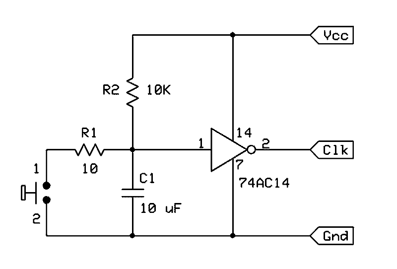
After initial use of the device, I increased R2 to 22K to slow down the device to compensate for my spastic hands.
With Ø2 contretemps out of the way, I was able to make some progress in actually debugging my contraption. POC V2 is not yet at the functioning state, so it's not quite time to put on the loud music, break out the beer and start the party. However, I'm working this in stages and so far, two hurdles have been cleared.
- The first hurdle was to determine if it was possible to select the QUART and access a register. The setup was to remove the MAX248 transceiver from the socket and burn a ROM that did nothing but repeatedly perform a read on the QUART's channel A receiver FIFO. I started with this ROM by single-stepped the clock and observed that when the LDA IO_ACIA+NX_RHRA instruction was executed (RHR means "receiver holding register," which is NXP-speak for the FIFO), the QUART's /CEN (chip enable) input went low, showing that selection was occurring during Ø2 low after VDA went high, which is correct logic. At that time, RWB and /RD (read data) were also high, which is also correct—/RD is generated by the CPLD and is the expression !(RWB & Ø2).
On the next step of the clock, Ø2 was high, /CEN was still low and /RD was pulled, the latter correct for a read cycle. I noted at that time that the data bus had a random pattern on it (D0-D7 had $00 when Ø2 was low, i.e., the bank address), which would be logical, given that the FIFO would contain undefined content immediately following power-up. On the next clock step, Ø2 was again low, /RD was high and /CEN was high, which was correct. I had proved that I could complete a read cycle on the QUART. Following the single-step testing, I installed a 2 MHz oscillator (Ø2 = 1 MHz). and powered up. Observation of the relevant signals indicated that the QUART was being repeatedly selected and a read operation was being repeatedly performed. - The second hurdle was to see what would happen with multiple writes to the channel A transmitter FIFO. I burned another ROM that wrote enough setup into the QUART to enable the transmitter and then repeatedly write $A5 into it. I also connected a second logic probe to the QUART's TxDA (channel A transmitter) output, which is a TTL-level signal output to the MAX248. TxDA is supposed to be high (mark condition) when the transmitter is enabled and quiescent, which it was right after reset. Again, I manually cycled the clock while watching /CEN and /WD (write data) as the MPU progressed.
When the STA IO_ACIA+NX_THRA instruction was executed and while Ø2 was low, VDA was high, RWB was low, /WD was high—/WD is generated by the CPLD and is the expression !(!RWB & Ø2)—and /CEN went low. All of that was correct. On the next clock step, Ø2 went high and /WD went low. At that time, I saw a brief burst of activity on the logic probe connected to TxDA, which meant the QUART had transmitted something. The pattern on D0-D7 was %10100101, which is $A5, the test value. Following the activity, TxDA returned to the mark condition, as it should.
I then replaced the single-stepper with the oscillator and powered up. There was continuous activity at TxDA for a few seconds, which would have corresponded to the write some data and halt code I had burned into the EPROM. Following that test, I put the MAX248 back into the socket and connected POC V2 to my console terminal, with my RS-232 tester in the circuit so I could watch the signals. At power-up, all RS-232 signals, other than RI (ring in, which is not used), showed voltage present. After releasing the reset line, I saw a burst of activity on the tester's RD indicator (receive data—the tester was "backwards" in the circuit, so RD is from the terminal's perspective), indicating something was being transmitted to the terminal. The terminal's display, which had previously blanked from a "no activity" timeout, woke up. However, there was no other evidence of data being received, even though $A5 should have caused the terminal to display % (italicized percent).
The other possibility is the bit patterns for baud rate and format are being written into the wrong registers, either due to a register decoding logic error or due to a typo somewhere in one of the assembler INCLUDE files that contains the 28C94 data.
Since software is easier to fix than hardware and I have no reason to further suspect hardware at this point, it's time to fire up the assembler.
x86? We ain't got no x86. We don't NEED no stinking x86!
- BigDumbDinosaur
- Posts: 9425
- Joined: 28 May 2009
- Location: Midwestern USA (JB Pritzker’s dystopia)
- Contact:
Re: POC VERSION TWO: Debugging Update
BigDumbDinosaur wrote:
Based upon the above testing, it appears my CPLD logic has some degree of correctness to it, the QUART is not comatose and I can send something to the console terminal. I'm inclined to think that right now I must have a baud rate error, formatting error, or both, in the serial data stream...Since software is easier to fix than hardware and I have no reason to further suspect hardware at this point, it's time to fire up the assembler.
At one point during the design of POC V2, I had considered using two 28L92s instead of the single 28C94, but nixed that idea because I don't have enough outputs on the ATF1504AS CPLD. Also, there was the matter of PCB real estate...
x86? We ain't got no x86. We don't NEED no stinking x86!
- GARTHWILSON
- Forum Moderator
- Posts: 8773
- Joined: 30 Aug 2002
- Location: Southern California
- Contact:
Re: POC VERSION TWO: Debugging Update
BigDumbDinosaur wrote:
Also, there was the matter of PCB real estate... 
http://WilsonMinesCo.com/ lots of 6502 resources
The "second front page" is http://wilsonminesco.com/links.html .
What's an additional VIA among friends, anyhow?
The "second front page" is http://wilsonminesco.com/links.html .
What's an additional VIA among friends, anyhow?
- BigDumbDinosaur
- Posts: 9425
- Joined: 28 May 2009
- Location: Midwestern USA (JB Pritzker’s dystopia)
- Contact:
POC VERSION TWO: Debugging Update
GARTHWILSON wrote:
BigDumbDinosaur wrote:
Also, there was the matter of PCB real estate... 
I'll tell you...I'm really tempted to whip up a design using the ATF1508AS and two (maybe four) 29L92s. Those UARTs work great and with 16 deep FIFOs, they don't bang away at the MPU with IRQs like some other UARTs. However, POC V2 has to be made operative before anything new can be designed.
x86? We ain't got no x86. We don't NEED no stinking x86!
Re: POC VERSION TWO: Debugging Update
BigDumbDinosaur wrote:
I'm stumbling around with this, partially because the 28C94 data sheet has errors and inconsistencies, and is not well organized. I been trying to find other documentation on the part or some application notes, but so far the Internet has failed me. Almost makes me wish I had used the (more complicated) 28L194, whose data sheet is an easier read and is better organized. However, the 28L194 operates on a synchronous bus, which I'm not sure can be properly implemented with the 65C816.
Regarding the 28C94 in your board: Have you tried the simplest of all interactions with the 28C94? It looks like you should be able to toggle the general purpose output pins with just a few register configurations.
IOPCRA = 01000000
Then toggle bit 5 of OPRab.
I've never used this part and am just reading the datasheet like the next guy but it looks like it should work? Could you point out some of the inconsistencies? Maybe we can help "resolve" them.
If I was a betting bloke I'd put at least $5 on your problem being down to the baud rate config or something similar.
BTW regarding your test pattern. Why not just use a 7 bit ASCII character? My favourite is 0x2A, the asterisk.
Quote:
At one point during the design of POC V2, I had considered using two 28L92s instead of the single 28C94, but nixed that idea because I don't have enough outputs on the ATF1504AS CPLD. Also, there was the matter of PCB real estate... 
8 bit fun and games: https://www.aslak.net/
- BigDumbDinosaur
- Posts: 9425
- Joined: 28 May 2009
- Location: Midwestern USA (JB Pritzker’s dystopia)
- Contact:
Re: POC VERSION TWO: Debugging Update
Aslak3 wrote:
I'm confused; the 68K DTACK-mchanism is classed as an asynchronous bus, but busses like the 6502 are considered synchronous? If the 28L194 operates in a 68K style, it can probably be made to work by delaying the Chip Select until after Read or Write have been asserted. I used this trick successfully with the SC16C654 on my board which I configured in 68K mode because it required less glue pins.
In any case, x86 mode is somewhat easier with the 65C816, due to the independent control of the read/write functions. In 68K mode, read/write works along the line of 65xx silicon, which make qualifying a read against the Ø2 clock impossible without extra silicon—unlike the 65C22, for example, the 28C94 doesn't know that the data bus is not data during Ø2 low.
Quote:
Regarding the 28C94 in your board: Have you tried the simplest of all interactions with the 28C94? It looks like you should be able to toggle the general purpose output pins with just a few register configurations.
Quote:
I've never used this part and am just reading the datasheet like the next guy but it looks like it should work? Could you point out some of the inconsistencies? Maybe we can help "resolve" them.
Quote:
If I was a betting bloke I'd put at least $5 on your problem being down to the baud rate config or something similar.
Quote:
BTW regarding your test pattern. Why not just use a 7 bit ASCII character? My favourite is 0x2A, the asterisk.
Then when it works you can say you are "seeing stars". This might be an indicator that I need to get out more.
x86? We ain't got no x86. We don't NEED no stinking x86!
Re: POC VERSION TWO: Debugging Update
BigDumbDinosaur wrote:
Go to page 17 for an example. In the right column, the data sheet abruptly goes from describing the layout of the clock select register to the command register, obviously an editing error.
Quote:
Also, the baud rate table (table 6) is a bit confusing, as it mentions BRG RATE = LOW and BRG RATE = HIGH (BRG meaning baud rate generator), but there is no immediate clue as to which register is used to set the baud rate generator rate (it's register %101101).
Quote:
Furthermore, there is are registers %101110 and %101111 listed in table 1 on page 6, but no satisfactory explanation for what they do.
I find most NXP datasheets terse and difficult to chew through, but this one doesn't seem excessively bad, that crappy CR, CSR, CR mistake notwithstanding.
8 bit fun and games: https://www.aslak.net/
- BigDumbDinosaur
- Posts: 9425
- Joined: 28 May 2009
- Location: Midwestern USA (JB Pritzker’s dystopia)
- Contact:
Re: POC VERSION TWO: Debugging Update
Aslak3 wrote:
BigDumbDinosaur wrote:
Go to page 17 for an example. In the right column, the data sheet abruptly goes from describing the layout of the clock select register to the command register, obviously an editing error.
None of the NXP data sheets are particularly well-written. This one seems to have set a new standard in that regard.
Quote:
Quote:
Also, the baud rate table (table 6) is a bit confusing, as it mentions BRG RATE = LOW and BRG RATE = HIGH (BRG meaning baud rate generator), but there is no immediate clue as to which register is used to set the baud rate generator rate (it's register %101101).
Quote:
...hex 00 for LOW and hex 01 for HIGH? I'm not sure what's confusing there.
Quote:
Quote:
Furthermore, there is are registers %101110 and %101111 listed in table 1 on page 6, but no satisfactory explanation for what they do.
Quote:
I find most NXP datasheets terse and difficult to chew through, but this one doesn't seem excessively bad, that crappy CR, CSR, CR mistake notwithstanding.
x86? We ain't got no x86. We don't NEED no stinking x86!
- BigDumbDinosaur
- Posts: 9425
- Joined: 28 May 2009
- Location: Midwestern USA (JB Pritzker’s dystopia)
- Contact:
Re: POC VERSION TWO: Debugging Update
BigDumbDinosaur wrote:
Also, the baud rate table (table 6) is a bit confusing, as it mentions BRG RATE = LOW and BRG RATE = HIGH (BRG meaning baud rate generator), but there is no immediate clue as to which register is used to set the baud rate generator rate (it's register %101101).
Aslak3 wrote:
It looks like it's register 101101...
Quote:
Quote:
Furthermore, there is are registers %101110 and %101111 listed in table 1 on page 6, but no satisfactory explanation for what they do.
Anyhow, these changes succeeded producing some output and my simple test loop now writes a series of characters to the terminal screen, albeit slowly, despite the interface running at 115.2 Kbps. At least it's some progress.
x86? We ain't got no x86. We don't NEED no stinking x86!
Re: POC VERSION TWO: Debugging Update
BigDumbDinosaur wrote:
I wrote into register %101110, which is tersely described as "Set X1/CLK divide by two (use when X1 is < 4 Mhz)". As I am using a 3.6864 MHz oscillator to drive the X1 clock, it would seem that writing into that register would be appropriate. This register and the one that follows it are strange, as nothing in previous data sheets mentioned setting anything to account for the X1 frequency (up to 8 MHz is supported by the 26C92, 28L92 and 28C94). The other logical X1 frequency would be 7.3728 MHz, which would effectively double all the standard baud rates.
Quote:
Anyhow, these changes succeeded producing some output and my simple test loop now writes a series of characters to the terminal screen, albeit slowly, despite the interface running at 115.2 Kbps. At least it's some progress.
When you say slowly, do you mean each character appears with a gap, but the baud rate at the terminal end is 115.2K? If so, this is odd indeed and could only be that your polling for FIFO empty is being delayed somehow?
8 bit fun and games: https://www.aslak.net/
- BigDumbDinosaur
- Posts: 9425
- Joined: 28 May 2009
- Location: Midwestern USA (JB Pritzker’s dystopia)
- Contact:
Re: POC VERSION TWO: Debugging Update
Aslak3 wrote:
That reads like it should be "> 4Mhz". Hmm. Are 7.328MHz crystals common?
7.3728 MHz is a standard oscillator frequency. Mouser lists about 160 stock items in that frequency.
Quote:
BigDumbDinosaur wrote:
Anyhow, these changes succeeded producing some output and my simple test loop now writes a series of characters to the terminal screen, albeit slowly, despite the interface running at 115.2 Kbps. At least it's some progress.
When you say slowly, do you mean each character appears with a gap, but the baud rate at the terminal end is 115.2K? If so, this is odd indeed and could only be that your polling for FIFO empty is being delayed somehow?
Adding insult to injury, I changed my test code to copy the test character string from RAM to ROM and then used the RAM copy to write it repeatedly to the terminal. In fact, I did this from addresses $002000, $00D800, $01D800 and $0FFFF0, proving that memory decoding is working as it should. That last address is decimal 1,048,560, 16 bytes shy of POC V2's 1 MB address limit. I also tested with a 30 MHz oscillator on board, which runs Ø2 at 15 MHz. Works like a charm!
Now I have to get busy and slap together a BIOS.
x86? We ain't got no x86. We don't NEED no stinking x86!
Re: POC VERSION TWO: Debugging Update
BigDumbDinosaur wrote:
She's off life-support. ...
Now I have to get busy and slap together a BIOS.
A question about your BIOS and your QUART driver. Appreciate that this is probably OT. I assume you are planning on an interrupt-based driver. Have you implemented transmit interrupts in your previous BIOS? I have really, really struggled to get my head around this topic in my project. Rx interrupts are conceptually simpler - you just get an interrupt when you have some data to read. I have implemented these and am very pleased with the result; tasks waiting for an interrupt do not get scheduled until they Rx something. But transmit interrupts need some mental gymnastics I can't quite manage - your main code is interrupt when what has been sent has finished sending, but it is the main code which started the sending in the first place?! I just can't quite get this working. Any advice?
8 bit fun and games: https://www.aslak.net/
- BigDumbDinosaur
- Posts: 9425
- Joined: 28 May 2009
- Location: Midwestern USA (JB Pritzker’s dystopia)
- Contact:
Re: POC VERSION TWO: Debugging Update
Aslak3 wrote:
BigDumbDinosaur wrote:
She's off life-support. ...
Now I have to get busy and slap together a BIOS.
Quote:
A question about your BIOS and your QUART driver. Appreciate that this is probably OT. I assume you are planning on an interrupt-based driver. Have you implemented transmit interrupts in your previous BIOS?
Quote:
I have really, really struggled to get my head around this topic in my project...But transmit interrupts need some mental gymnastics I can't quite manage...
You start out with the transmitter or its IRQ disabled. A flag¹ is set somewhere in memory to tell your driver that TxD is disabled. That's the initial setup, which should occur at power-on or reset.
When something has to be transmitted, the foreground part of your driver buffers the byte and then examines the TxD disabled flag. If TxD is disabled, the foreground clears the flag, enables the transmitter (or its IRQ) and returns to the caller. Shortly after enabling TxD, the UART will generate a TxD IRQ. If TxD is already enabled the foreground doesn't have to do anything and just returns to the caller.
Your interrupt service routine (ISR), after determining that an IRQ was caused by the UART's transmitter, would read a byte from the transmit buffer and write it to the UART. In the case of UARTs with FIFOs, such as the 28L91 or 16650, you would repeat the read-buffer/write-UART loop until either the UART says its TxD FIFO is full or the TxD buffer becomes empty.
If the UART says its FIFO is full your ISR simply terminates. Later on, the UART will again produce a TxD IRQ when the FIFO has emptied. The steps described in the previous paragraph would be repeated.
If the buffer becomes empty, you disable TxD or its IRQ and set the flag saying so, as was done during initialization. Following that, your ISR would terminate.
Hope this description helps to clear it up.
———————————————————————————————
¹In the case of a multi-channel UART, a single byte can be used as the TxD disabled flag, using individual bits to represent each transmitter in the UART.
x86? We ain't got no x86. We don't NEED no stinking x86!
Re: POC VERSION TWO
Congratulations with POC 2 getting to work, and lots of fun with programming!
Marco