WDC’s naming of those signals is the convention, since WDC was the entity that developed the 65C02. Rockwell, Synertek et al were licensees.
As far as I know MOS Technology was founded in 1969, later in 1978 WDC was founded (by a former MOS Technology employee), so it seems more likely to me than that WDC did not set, but changed the standard.
Compared to NMOS 6502s which predated WDC, yes, L0uis.m, it's true that the manufacturer's terminology in reference to the clock pins did change (and also the recommendation of what to do with those pins).
Understanding the recommended connection is moderately important. (But I don't see much point in debating whether one pin
naming convention or the other should be considered "correct" or "standard." Certainly WDC's convention is standard for WDC, but I wouldn't bother pursuing the point any further.)
I do kinda understand why WDC made the naming change, though.
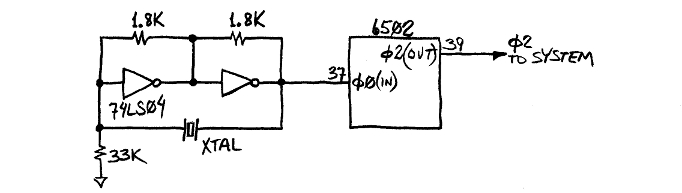
For technical reasons, they'd decided that having their CPU be the middleman, and thus the source of Phi2 for other devices in the system, was not the best arrangement. Instead they suggested that it'd be better if all devices in the system -- including the CPU -- should simply accept Phi2 as an input.
And I can see potential for confusion if the name of pin 37 were
not changed. Some folks would find it strange that the signal driving their VIA's Phi2 input would also connect to CPU pin 37... whose name cites Phi
0.

I suspect that's why WDC renamed pin 37 as PHI2. (They also stopped using the Φ character in all three of the pin names, substituting PHI instead.)
It's important to be clear that the pin
functions didn't change. Pin 37 is always an input, and pin 39 and pin 3 are always outputs, although the latter two won't necessarily get used (at least not externally -- but the internal signals fed to pin 39 and pin 3 do get used internally by the CPU).
Finally, it's perhaps a simplification for me to have drawn inverters to represent the internal circuitry, as there may be some degree of pulse shaping going on as well. But inverters do accurately give the general idea.
-- Jeff


