Page 3 of 6
Re: POC COMPUTER VERSION TWO: A New Direction
Posted: Sat Aug 14, 2021 2:33 am
by floobydust
Simple motto... "life's too short to drink cheap wine, ...
Speaking of cheap wines: I make my own wines. Have a small vineyard that produces 50-75 gallons of wines a year. I'll be busily harvesting grapes and making wine in 3 weeks.
I also make my own (cheap) labels by stick a piece of duct tape over the bottle. I'm proud of the cheap labels; my place is known as "Duct Tape Winery".
Bill
Wow...it never ceases to amaze me at what a diverse and talented group of folks out here... us ole guys... we got game! You'll have to post some pics of your wine making!
Re: POC COMPUTER VERSION TWO: A New Direction
Posted: Sat Aug 14, 2021 7:45 am
by BigDumbDinosaur
Wow...it never ceases to amaze me at what a diverse and talented group of folks out here... us ole guys... we got game!
Yep! I'm so talented I can talk and belch at the same time. 
Re: POC COMPUTER VERSION TWO: A New Direction
Posted: Sat Aug 14, 2021 6:12 pm
by barrym95838
Yep! I'm so talented I can talk and belch at the same time.
Running two simultaneous data streams from a single I/O port? As long as it's intentional and the intended receiver is able to successfully decode, I think that should definitely qualify as a feature and not a bug.
Re: POC COMPUTER VERSION TWO: A New Direction
Posted: Sun Aug 15, 2021 7:51 pm
by BigDumbDinosaur
Woo-Hoo! PCBs in shortly then...
Got the ship notice from the board house yesterday. Now it's up to the courier...
Meanwhile, I've been fooling around with the CPLD code. I decided to go ahead and make I/O decoding more granular, which exposes more RAM between the top of the I/O block and the bottom of ROM. This version also has the ability to switch out ROM and expose the RAM underneath it. When ROM is in, a write to a ROM address will bleed through to RAM.
It all simulates as expected...which doesn't guarantee that it will actually work. 
Code: Select all
/*
* * * * * * * * * * * * * * * * * * * * * * * * * * * * * * * * * * * * * * * * * *
*                                                                                 *
*                 W65C816S PROOF OF CONCEPT SINGLE-BOARD COMPUTER                 *
*                                                                                 *
* =============================================================================== *
*                                                                                 *
*        Copyright (c)2021 by BCS Technology Limited.  All rights reserved.       *
*                                                                                 *
* Permission is hereby granted to use, copy, modify and distribute this software, *
* provided this copyright notice remains unaltered in the source code and  proper *
* attribution is given.  Redistribution, in any form, must be at no charge to the *
* end user.  This code or any part  thereof, including any derivation, MAY NOT be *
* incorporated into any package intended for sale unless written permission to do *
* so has been granted by the copyright holder.                                    *
* ------------------------------------------------------------------------------- *
* THERE IS NO WARRANTY OF ANY KIND WITH THIS SOFTWARE.                            *
*                                                                                 *
* While it is believed that all code will perform as intended,  the user  assumes *
* all risk in connection with the incorporation of this software into any system. *
*                                                                                 *
* * * * * * * * * * * * * * * * * * * * * * * * * * * * * * * * * * * * * * * * * *

* * * * * * * * * *
* VERSION HISTORY *
* * * * * * * * * *

Ver    Rev Date    Revision
--------------------------------------------------------------------------------
0.1.0  2021/06/28  Original version.
--------------------------------------------------------------------------------
*/

Name        logic;
PartNo      C106280001;
Date        2021/06/28;
Revision    0.1.0;
Designer    BDD;
Company     BCS Technology Limited;
Assembly    POC V2.0;
Location    U6;
Device      f1504ispplcc44;

property	 atmel {cascade_logic  on       };
property	 atmel {err_file       logic.err};
property	 atmel {fast_inlatch   on       };
property	 atmel {fold           off      };
property	 atmel {foldback_logic on       };
property	 atmel {logic_doubling off      };
property	 atmel {optimize       on       };
property	 atmel {output_fast    off      };
property	 atmel {pin_keep       off      };
property	 atmel {preassign      keep     };
property	 atmel {security       off      };
property	 atmel {soft_buffer    on       };
property	 atmel {xor_synthesis  on       };

/*
==============================================
MACHINE ARCHITECTURE IMPLEMENTED IN THIS LOGIC
==============================================

	        +--------------------------+ $01FFFF
	        |                          |
	        |                          |
	        |                          |
	        |  Extended RAM  (64 KB)   |
	        |                          |
	        |                          |
	        |                          |
	        +--------------------------+ $010000
	        |                          |
	        |        ROM (12 KB)       |
	        |                          |
	        +--------------------------+ $00D000
	        |                          |
	        |     SYSRAM (3.25 KB)     |
	        |                          |
	        +--------------------------+ $00C300
	        |                          |
	        |       HMU (0.25 KB)      |
	        |                          |
	        +--------------------------+ $00C200
	        |                          |
	        |      IODEV (0.5 KB)      |
	        |                          |
	        +--------------------------+ $00C000
	        |                          |
	        |                          |
	        |      BASRAM (48 KB)      |
	        |                          |
	        |                          |
	        +--------------------------+ $000000
	             1 KB = 1024 bytes

	      ---------------------------------
	      | I/O MAP (10 bits of decoding) |
	      ---------------------------------
	           +--------------------+ $00C200
	           |                    |
	           |      RESERVED      |
	           |                    |
	           +--------------------+ $00C1C0
	           |                    |
	           |        XIO6        | Expansion Chip Select
	           |                    |
	           +--------------------+ $00C180
	           |                    |
	           |        XIO5        | Expansion Chip Select
	           |                    |
	           +--------------------+ $00C140
	           |                    |
	           |        XIO4        | Expansion Chip Select
	           |                    |
	           +--------------------+ $00C100
	           |                    |
	           |        XIO3        | Expansion Chip Select
	           |                    |
	           +--------------------+ $00C0C0
	           |                    |
	           |        XIO2        | vQUART Channel IRQs
	           |                    |
	           +--------------------+ $00C080
	           |                    |
	           |        XIO1        | DUART #2 (channels C & D)
	           |                    |
	           +--------------------+ $00C040
	           |                    |
	           |        XIO0        | DUART #1 (channels A & B)
	           |                    |
	           +--------------------+ $00C000

                            Signal            Type    Function
=============================================================================*/
pin  33                   = A6;            /* input   address line           */
pin  34                   = A7;            /* input   address line           */
pin  21                   = A8;            /* input   address line           */
pin  24                   = A9;            /* input   address line           */
pin  25                   = A10;           /* input   address line           */
pin  26                   = A11;           /* input   address line           */
pin  27                   = A12;           /* input   address line           */
pin  28                   = A13;           /* input   address line           */
pin  29                   = A14;           /* input   address line           */
pin  31                   = A15;           /* input   address line           */
pin   5                   = A16;           /* output  address line           */
pin  39                   = D0;            /* input   unbuffered data line   */
pin  36                   = DB0;           /* input   buffered data line     */
pin  43                   = PHI1;          /* input   system clock (phase 1) */
pin   2                   = PHI2;          /* input   system clock (phase 2) */
pin   6                   = !RAM;          /* output  RAM chip select        */
pin  19                   = !RD;           /* output  read data              */
pin   1                   = RESB;          /* input   system reset           */
pin  18                   = !ROM;          /* output  ROM chip select        */
pin  44                   = RWB;           /* input   MPU read/write         */
pin  41                   = VDA;           /* input   valid data address     */
pin  40                   = VPA;           /* input   valid program address  */
pin  20                   = !WD;           /* output  write data             */
pin   4                   = !WSE;          /* output  clock stretch control  */
pin  [8,9,17,11,12,14,16] = ![XIO0..6];    /* output  I/O chip selects       */


/*
=========================
BURIED LOGIC DECLARATIONS
=========================
*/
pinnode   = extram;                                   /* extended address latch     */
pinnode   = hmu0;                                     /* hardware management latch  */
pinnode   = hmusel;                                   /* 1 = HMU selected           */
pinnode   = iosel;                                    /* 1 = I/O device selected    */
pinnode   = romsel;                                   /* 1 = ROM selected           */
pinnode   = vab;                                      /* 1 = valid address present  */

/*
==================
FIELD DECLARATIONS
==================
*/
field addr     = [A15..A6];                           /* effective address LSW */

/*
==================
INTERMEDIATE LOGIC
==================
*/
hmu0.AR         = !RESB;

extram.LE       = PHI1;
extram.L        = D0;
hmusel          = extram:0 & addr:['h'C20x];
iosel           = extram:0 & addr:['h'C0xx..C1Fx];
romsel          = extram:0 & addr:['h'D0xx..FFxx] & !hmu0 & RWB;
/*
	--- A write to ROM goes to RAM at the same address.
*/
vab             = (VDA # VPA) & RESB;

/*
======
INPUTS
======
*/
hmu0.LE    =  hmusel & !RWB & PHI2 & vab;
hmu0.L     =  hmusel & !RWB & PHI2 & vab & DB0;

/*
=======
OUTPUTS
=======
*/
A16             = extram & RESB;
DB0.OE          = hmusel & RWB & PHI2 & vab;
DB0             = hmusel & RWB & PHI2 & vab & hmu0;
RD              = RWB & PHI2 & vab;
WD              = !RWB & PHI2 & vab;
WSE             = iosel # romsel & vab;
RAM             = !(hmusel # iosel # romsel) & vab;
ROM             = romsel & vab;
XIO0            = iosel & addr:['h'x00x] & vab;
XIO1            = iosel & addr:['h'x04x] & vab;
XIO2            = iosel & addr:['h'x08x] & vab;
XIO3            = iosel & addr:['h'x0Cx] & vab;
XIO4            = iosel & addr:['h'x10x] & vab;
XIO5            = iosel & addr:['h'x14x] & vab;
XIO6            = iosel & addr:['h'x18x] & vab;
/*
	--- $00C1C0 - $00C1FF reserved for future expansion.
*/

/* * * * *   E N D   O F   F I L E   * * * * */
Re: POC COMPUTER VERSION TWO: A New Direction
Posted: Mon Aug 16, 2021 12:06 pm
by floobydust
Nice... my last order of some odd parts came from China... they made it over in about a week. It was also free shipping on a couple interface PCBs (one tiny connector on it) and some FPC cables. Oddly, the package had USPS shipping from Illinois. In any case, hope they get here sooner.
Re: POC COMPUTER VERSION TWO: A New Direction
Posted: Mon Aug 16, 2021 3:28 pm
by BigDumbDinosaur
Nice... my last order of some odd parts came from China... they made it over in about a week. It was also free shipping on a couple interface PCBs (one tiny connector on it) and some FPC cables. Oddly, the package had USPS shipping from Illinois. In any case, hope they get here sooner.
The PCB order is coming in two shipments. The stencil was shipped separately from the PCBs, probably because stencils are relatively fragile and thus require different packaging.
As for the USPS thing, that's not uncommon with overseas shipments. The courier may not have the facilities for local handling your area. International shipments that travel by air will arrive at the nearest major airport for customs clearance—in your case, it sounds as though it was O'Hare in Chicago. The courier will then turn the shipment over to the postal service to cover the domestic part of handling the package. Given the labor problems that USPS has, that part of the process is probably the riskiest. 
Re: POC COMPUTER VERSION TWO: A New Direction
Posted: Mon Aug 16, 2021 5:51 pm
by Martin A
Has something changed in the clocking ?
The schematic has PHI1 to PIN 2 and PHI2 on PIN 43
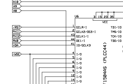
- Schematic snip
- Screenshot 2021-08-16 184558.jpg (23.92 KiB) Viewed 1999 times
The CUPL seems to have them the other way around:
Code: Select all
pin  43                   = PHI1;          /* input   system clock (phase 1) */
pin   2                   = PHI2;          /* input   system clock (phase 2) */
Re: POC COMPUTER VERSION TWO: A New Direction
Posted: Mon Aug 16, 2021 8:05 pm
by BigDumbDinosaur
Has something changed in the clocking ?
The schematic has PHI1 to PIN 2 and PHI2 on PIN 43
The CUPL seems to have them the other way around:
Code: Select all
pin  43                   = PHI1;          /* input   system clock (phase 1) */
pin   2                   = PHI2;          /* input   system clock (phase 2) */
You, sir, are commended for your powers of observation.
I changed that around after I had posted the schematic and board layout. The CUPL code is correct.
Re: POC COMPUTER VERSION TWO: A New Direction
Posted: Sat Aug 21, 2021 5:39 am
by BigDumbDinosaur
Well, I received the stencil, but no sign of the PCBs. They were supposed to show up Friday.
Re: POC COMPUTER VERSION TWO: A New Direction
Posted: Sat Aug 21, 2021 8:29 pm
by Martin A
You, sir, are commended for your powers of observation.
Well..... I have a reason for following along the design closely:
 Viewed 1929 times")
- POC2 and a bit
The lower 2/3 of the board is basically the POC2, the upper third has all the I/O from a recent Z180 build. Left to right Wiz810s Ethernet header, 82C55 & IDE header, 2 chip VGA Video solution, and dumb keyboard port.
Ive been looking at building a 65816 board with BBC basic for a while, your clock stretching circuit solved the problem of limiting the speed to that of the slowest I/O components, the Z180 didn't have that problem as it has a build in wait state generator. The big advantage the 65816 has over the Z180, is no MMU to deal with and no restricted 64k visible at any one time memory.
The I/O from the Z180 build needs 4 I/O selects that also fits within the POC2 7 device memory map. So basically with the CPU, clock stretching, 128k ram and CPLD memory mapper, I had 70% of a POC2 anyway so I added provision for the serial connections.
There are differences of course, to make all 128k ram visible as well as 128k rom a 4 bank memory map is defined, and of course the video ram has its place in the memory map. However, in theory, if the memory mapping CPLD code were tweaked and the serial components fitted it ought to be compatible, if slower.
HC and HCT parts and a 70ns flash for rom limit it to 10mhz at the moment for developoing the basic I/O drivers. The 24mhz oscillator was a step to far without extending the wait stating to the rom.
Re: POC COMPUTER VERSION TWO: A New Direction
Posted: Mon Aug 30, 2021 5:14 am
by BigDumbDinosaur
Well, I received the stencil, but no sign of the PCBs. They were supposed to show up Friday.
 The board is electrically correct but the footprint I used for the 'AC245 transceiver was wrong. It has the right number of lands but is the wrong package width. Below is the incorrect PCB layout. The mistake is with U4, which is located at the southwest corner of the 65C816 socket.
 Viewed 1888 times")
- V2.0 PCB w/Wrong Component Footprint
I thought it might be possible to scab the transceiver in place by reforming the leads, but that won't fly due to the part being too wide relative to the layout footprint, as well as being jammed up close to the 65C816's socket.
Having discovered this little contretemps, my only recourse was to fix the board layout and place another order with JLCPCB. Below is the repaired layout. Since I was forced to a do-over, I made some other layout changes as well. Let's see if any of you who read this can spot those changes.
 Viewed 1888 times")
- V2.0 PCB w/Right Component Footprint
Supposedly, I'll have the new PCBs and stencil on Thursday. It really tees me off when I make a boneheaded blunder like that. 
Oh, what the hell: it's only money! 
Re: POC COMPUTER VERSION TWO: A New Direction
Posted: Mon Aug 30, 2021 5:43 am
by GARTHWILSON
Would the '245 fit if you were to J-lead it? Hopefully the leads would not break in the effort. I know there was some kind of tool to do a good job of it very quickly, but I've never seen one.
I know you said you already ordered the revised board though.
Re: POC COMPUTER VERSION TWO: A New Direction
Posted: Mon Aug 30, 2021 6:51 am
by BigDumbDinosaur
Would the '245 fit if you were to J-lead it? Hopefully the leads would not break in the effort. I know there was some kind of tool to do a good job of it very quickly, but I've never seen one.
I know you said you already ordered the revised board though.
Of course, the stencil I got with the bad boards is useless as well. I ordered a new stencil to go with the new boards so I can try my hand at reflowing a second unit once the prototype has been built and made functional.
This is the first board layout that I have goofed up in over 10 years. Maybe old age is to blame.
Re: POC COMPUTER VERSION TWO: A New Direction
Posted: Mon Aug 30, 2021 9:03 am
by floobydust
Ouch! That hurts.... more fancy coasters for the workshop it seems.
Re: POC COMPUTER VERSION TWO: A New Direction
Posted: Mon Aug 30, 2021 11:02 am
by J64C
Gotta post pics of the boards anyway though! Can’t leave us hanging.
