Page 3 of 6
Re: Slower SRAM works but fast doesn't????
Posted: Tue Jun 19, 2018 10:37 pm
by dolomiah
Hi GaBuZoMeu
Ok so I was going to do yet another edit to my post this evening but you got in there with a comment, so will do a reply instead

The /WE line is unqualified - direct from 65c02. So /CE is key! I have found my address decoding notes - a table of the connections to the three 74HCXX logic chips I utilised. Hopefully within a couple of days, I will draw this up for folks to prod at
Re: Slower SRAM works but fast doesn't????
Posted: Tue Jun 19, 2018 11:10 pm
by BillO
I don't like /CE going high before /WE. In the other thread this was identified as an undefined condition.
We also discussed on that thread that both /WE and /OE need to be qualified by Phi2.
/CE should
NOT be Phi2 qualified!
The 'reference design' noted by GaBuZoMeu is the place to start. The schematic as provided by BDD is:
Connect /WD to RAM /WE.
Connect /RD to both RAM and ROM /OE.
If you still have a problem, then we can look at the CPU delay to remove any propagation delay. The propagation delay trick is still new and relatively untested and, if valid, should only be needed where extreme speed is encountered, so we should go with the proven architecture first.
Re: Slower SRAM works but fast doesn't????
Posted: Wed Jun 20, 2018 1:28 am
by Dr Jefyll
I don't like /CE going high before /WE. In the other thread this was identified as an undefined condition.
Whoa, wha? I'm still getting up to speed on that second datasheet!

Are we talking about the same thing -- is it this TWR spec that's at issue? I think the reference point (red arrow) is intended to mark the end of the write operation, which is to say the point at which either /WE or /CE has gone high. They could've included a second diagram in which it's /CS rather than /WE which is first to go high, but it's unsurprising they skipped that. For me, the meaning of the TWR spec is, "you need to keep the address stable until the write ends, but not afterward."
Edit to add: TDW and TDH (near the bottom) use the same reference point, and I just noticed TDW is "Data Valid to end of write" and TDH is "data hold from end of write."
Re: Slower SRAM works but fast doesn't????
Posted: Wed Jun 20, 2018 2:02 am
by BillO
When I look at that diagram I see those hash marks. I'm inclined (being the lazy sot that I am) to believe they are that way for a reason. There are no hash marks beyond the rise of /WE. This leads me to believe that what their limited text on the matter means is, that /WE should rise either coincidental with /CE or sometime before - but not after. Otherwise they would have included the hash marks after the rise of /WE too.
I don't know what the circuitry in that particular chip is actually like, but in my experience these are the functions of those inputs:
A low level on /CE will enable power to the I/O and dynamic circuitry of the chip.
A low to high transition of /WE will enable latching of the data present at the transition.
From that, and the way the diagram is offered, if /CE rises before /WE, it turns off power to the I/O before the data can be properly latched.
Re: Slower SRAM works but fast doesn't????
Posted: Wed Jun 20, 2018 3:45 am
by Dr Jefyll
A low to high transition of /WE will enable latching of the data present at the transition.
Yup. It halts the copying that had been in progress, the "transparent" write (like when a 74xx373 is following the input data).
A low level on /CE will enable power to the I/O and dynamic circuitry of the chip.
Yes, and a
high level on /CE stops whatever might be happening (including a write).
This leads me to believe that what their limited text on the matter means is, that /WE should rise either coincidental with /CE or sometime before - but not after.
So did I misunderstand by supposing it's TWR that concerns you? Not sure I'm following you. Beyond what I already said I can only elaborate that the reference point with the red arrow has the words "end of write" associated with it -- and the Truth Table tells us what a write is. It's the condition defined by /CE and /WE both being low.
You're certainly right about this datasheet having "limited text on the matter."

A look at datasheets for comparable RAM products, or better yet an Application Note, might shed a clearer light.
-- Jeff
Re: Slower SRAM works but fast doesn't????
Posted: Wed Jun 20, 2018 3:54 am
by GARTHWILSON
Since I'm in one of my busier times at work these days, I have been paying only mild attention to this topic; and with a few minutes' search now, I have not been able to find which SRAM IC we're talking about. However, none of the ones I've dealt with were edge-triggered. You have to have the CE\ and WE\ both low to write, and the location holds whatever the processor is putting on the bus when those are both low. It can change any number of times before the final value before first of them rises. Whenever the first of those rises is when the door to the address location is closed so to speak, and the location latches whatever value was there at the end of the time that both CE\ and WE\ were low. The manufacturer usually has several diagrams showing different ways to do it. Jeff's diagram specifically says "Write cycle 2."
/CE should NOT be Phi2 qualified!
There's no problem in qualifying it with phase 2 unless you need the additional time before the rise of phase 2 when the address may already be valid. SRAM tends to be available in faster speeds than ROM or any of the I/O ICs on the board though, so that extra time is often not needed. If you're pushing the upper speed limit of the 65c02, the guaranteed advance address-valid time nearly disappears anyway.
Re: Slower SRAM works but fast doesn't????
Posted: Wed Jun 20, 2018 4:35 am
by BillO
Apparently dolomiah I'm all wrong.
I have little to offer other than to try the 'reference design'.
Apparently if you use that then timing is otherwise not an issue - anything goes and it's all good.
Good luck.
Re: Slower SRAM works but fast doesn't????
Posted: Wed Jun 20, 2018 7:15 am
by BigEd
For future reference, we have (by coincidence) had two threads going on at the same time both relating to glue logic and SRAM accesses:
We've also in the recent past had another thread relating to CMOS 6502s and trouble with clock skew, which again looks a bit like a glue logic problem and uses some of the same kinds of reasoning to get to the bottom of it:
Re: Slower SRAM works but fast doesn't????
Posted: Thu Jun 21, 2018 10:05 pm
by kakemoms
Just my 50cents on the original problem:
I have seen this problem before. Using fast components (as CPLDs and SRAM) can give confusion when connected to slow transition clocks. As several have already pointed out, skew or slow clock transitions can make a fast component switch several times in the voltage transition (period). For a 6502 bus this involves 24 lines, which will make it look like several memory accesses, and at best give an unstable system.
Remember that a 5MHz square clock with fast transitions will require a large bandwidth. Its the transition time, not the clock rate which becomes your enemy with fast SRAM.
As for the 70ns SRAM not working, that is a different problem and good answers were given by others (nothing to add).
Re: Slower SRAM works but fast doesn't????
Posted: Sat Jun 23, 2018 1:16 am
by Dr Jefyll
I'm a little startled to realize we're three pages into this thread and have yet to see a schematic! There've been some interesting points raised, and speculative comparisons with BillO's thread, but we haven't seen Dolomiah's glue/decode logic. I look forward to seeing that. Meanwhile here's more speculation:
Of course you cannot rely on using slow RAMs to mediate timing errors
.
Right, it's not reliable. But in practice a slow chip *can* mask a timing error, and I wonder if that explains Dolomiah's puzzling problem. Suppose the glue/decode logic is a little late in terminating the memory commands sent via /CE, /OE and /WE, causing a RAM write operation (say) to endure beyond the fall of Phi2 and into the first part of the following cycle. This is tolerable as long as tAH (the 65C02's Address Hold time) isn't exceeded, but after tAH expires the address bus begins its transition to whatever comes next -- and if the glue logic hasn't yet stopped asking for a write operation then that constitutes a spurious access.
If the spurious access lasts only a few ns it's plausible that a fast RAM chip might succeed in actually doing something -- something destructive, in this case! -- whereas a slow RAM chip might judiciously ignore the errant order!

This isn't the
only possible explanation of the behavior Doloniah reported, but it's a plausible one.
-- Jeff
Re: Slower SRAM works but fast doesn't????
Posted: Sat Jun 23, 2018 7:06 am
by GaBuZoMeu
Oh yeah,

you can try varying the voltage of the board. Lower voltages gives lesser drive to the MOSFETs causing higher R
DSON causing slower charge of internal and external Cs slowing signal down. If this happens mostly within the RAM and lesser in the decode logic you can use Vcc to vary the behavior from friendly to faulty

You may also try various temperatures...
Re: Slower SRAM works but fast doesn't????
Posted: Tue Jun 26, 2018 9:29 pm
by dolomiah
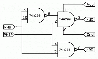
Hi Folks. Sorry for the delay, solid week at work and then away for a long weekend. I have converted my logic notes in to a diagram - see the attached mess which is realised by two 74XX00 NAND and one 74HCT04 (I have both LS and HCT NAND devices

)
I hope I have transcribed this correctly, as I know it works of course. I have included a couple of notes re the memory map and how many gates propagation delay to come up with the decode. The maximum is 4 gates of delay, which I guess could be in the order of 28-36ns. Also see that Phi2 is not used to qualify ROM or IO activation, only for RAM access.
I'm conscious that I haven't done an optimal job on this - I came up with this more than 3 years ago now (time flies) and it was my first go and more or less worked except I was using Phi2 for IO which I fixed after advice on this forum (only remembered now!).
The RAM device is a UM 621024 70ns device with the following control truth table (which I think is normal for many RAM chips):
/CE1 high or CE2 low is standby
/OE and /WE high is output disabled
/CE1 low, CE2 high, /OE low, /WE high is read
/CE1 low, CE2 high, /WE low is write (/OE don't care - in fact I have tied /OE low due to this)
The faster device is a UM 61512 15ns device, same truth table as above and same manufacturer (UMC). Did I mention that with the fast RAM, I can clock the 6502 at 5.38Mhz, 2.68Mhz or even 1.34Mhz and it is very glitchy. So this might be confirming theories that the RAM is too fast for a breadboard set up?
In addition: When the 3 enable lines to the 74xx138 select an IO device, Phi2 is then used for further qualification. For the 6551 and 2 times 6522, this is simply the same Phi2 as fed to the 6502. For the TMS9918, I have yet more logic to get a /CSR and /CSW signal.
In answer to a query about the clock frequencies - this has been dictated by my choice of using a TMS9918a which requires a 10.738Mhz clock. I have a 21.7727Mhz crystal and hence used this to divide by 2 for the TMS9918 and by 4 for the 6502.
I hate not being able to know definitively what is going on here - but maybe I have now given enough information for someone to work it out. However, if not, I will need to put it down to things like slew and breadboard noise - I need to move on with other things on my project!
As always, any views and advice welcome.
Re: Slower SRAM works but fast doesn't????
Posted: Tue Jun 26, 2018 9:43 pm
by BigDumbDinosaur
Hi Folks. Sorry for the delay, solid week at work and then away for a long weekend. I have converted my logic notes in to a diagram - see the attached mess which is realised by two 74XX00 NAND and one 74HCT04 (I have both LS and HCT NAND devices
)
Please post a monochrome version of your schematic for the benefit of your color-challenged readers (that would be me).
Re: Slower SRAM works but fast doesn't????
Posted: Tue Jun 26, 2018 9:59 pm
by Chromatix
As I think has already been noted in this thread, failing to qualify /OE with Phi2 could easily lead to glitches on the RAM output. Looking only at truth tables is problematic; you must also consider *when* input signals become valid and follow the chain of causality.
For example, with the ROM I would use ~(A14 & A15) which is valid early in the 6502's cycle, to drive /CE which typically has a relatively long latency to valid output, then use ~(Phi2 & RW) to drive /OE which typically has a much shorter latency. You can lead the same /OE signal to the RAM without needing to qualify it further, and this doesn't consume any extra gates - in fact, as you already use ~(A14 & A15) elsewhere, it saves one gate.
Your RAM /CS1 and CS2 logic also seems overcomplicated. I would generate a mask signal for your I/O area at $Bxxx (A15 & ~A14 & A13 & A12), and use that both as a pre-qualifier for both your I/O selectors and as one of your RAM chip-select signals. Feed the other one with (A14 | A15) or its complement, depending on which polarity is more convenient for the I/O mask.
In short, in general treat chip-select lines as address logic, and wire address decoding logic to them; treat output-enables and write-enables as control logic, and wire clock-qualified control signals to them.
Re: Slower SRAM works but fast doesn't????
Posted: Tue Jun 26, 2018 10:38 pm
by BillO
Also, assuming HCT logic, there could be as long as 48ns-88ns from address valid until the RAM is selected, then add to that the RAM access time of 15ns. I don't think this is a great situation, especially at 5.3MHz.
Also, as has been pointed out to me recently in a different thread, tying RAM /OE to ground can cause contention at the best of times - the faster the devices the more likely that is to occur.
You should seriously attempt to incorporate the 'reference design' that has been shown here for /WE and /OE (/RD).
In addition make some effort to simplify the /CE logic as much as possible and/or use faster gates to implement it.
Update: Monochrome version on schematic for BDD.