Page 3 of 4

Re: Fusion-6502 - The bridge between Old and New

Posted: Fri Sep 30, 2016 2:03 am
by Oneironaut
Ok, I have come up with the details on how my SPI Flash file system is going to work.
From here on, it will be referred to as FFS (Fusion File System).

Cartridges (SPI Flash Memories) are going to hold multiple programs and multiple data files, and the capacity will range from a few hundred megs to several gigs.
The flash will be written to via PC USB link directly to the Fusion system. A program I made to develop games and demos will do all the work.

There will be a single file called The TOC starting at location zero, and it will be a total of 64K in size.
In the TOC, there will be 41 byte entries defining files on the flash as so...

File Name : 32 Bytes (Fixed length alpha-numeric)
File Type : 1 Byte (0:Program / 1:Data)
File Start : 4 bytes (32 bit address value)
File Length : 4 Bytes (32 bit length value)

Since the TOC is 65536 bytes long, and a file entry is 41 bytes long, the TOC will be able to hold 1598 entries, which is more than enough.
I will probably just cap this to 1024 entries, since I like things to fit into byte sets.

All program Files will be exactly 64,768 Bytes in size, which is the full 64K memory space minus zero page, stack, and IO space.
Data files can be any length at all, up to 4,294,967,296 bytes in size due to the 32 bit addressing used.

When Fusion-64 boots, the FPGA will stuff the menu program into the 6502 program space, and then the 6502 will look for the SPI memory.
If a cartridge is present, it will read the TOC, and then stream all of the file names (programs only) to a place in the main working SRAM.
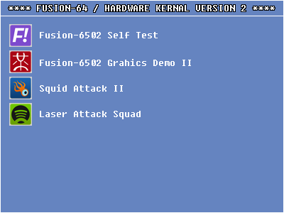
From there, the 6502 will draw up a boot menu where it will allow joystick navigation through the program files (not data files).

The user can then select a program and press fire to load it.
Once up and running, the program can refer to the loaded file table to gain location information on Data Files it may need to access.

There will be no writing from Fusion-64 to the Flash Memory, just reading.
The PC program will handle all writing of data, which will include compiled 6502 programs, sounds, and graphics.

I have had limited time, but managed to get text modes working, and added a Line Drawing function to the FPGA.
I will use lines and text to create a simple boot screen, which will also include a centering border and color test pattern.

I wanted to post more than just me yapping about this project, so here is the latest GPU function.
This is Verilog code that will draw a single pixel line from X1,Y1 to X2,Y2.
Although I hacked it about, one might still recognize Bresenham's line algorithm in here....

Code: Select all

///////////////////////////////////////////////////////////////////////////////////////////////////////////////////////////////////////////////////////////////////
////////// COMMAND 542 : DRAW LINE USING DRAWX1, DRAWY1, DRAWX2, DRAWY2
////////// DATA : LINE COLOR VALUE
///////////////////////////////////////////////////////////////////////////////////////////////////////////////////////////////////////////////////////////////////

// CALCULATE LINE DELTAS
if (COMMAND == 542 & COMSTEP == 1) begin
if (DRAWX1 > DRAWX2) DELTAX <= DRAWX1 - DRAWX2;
if (DRAWX1 < DRAWX2) DELTAX <= DRAWX2 - DRAWX1;
if (DRAWY1 > DRAWY2) DELTAY <= DRAWY1 - DRAWY2;
if (DRAWY1 < DRAWY2) DELTAY <= DRAWY2 - DRAWY1;
TEMPX <= DRAWX1;
TEMPY <= DRAWY1;
TEMPL <= 0;
COMSTEP <= 2;
end

// CALCULATE LINE STEPS
if (COMMAND == 542 & COMSTEP == 2) begin
if (DELTAX >= DELTAY) begin
LINELEN <= DELTAX;
DELTAQ <= (DELTAY >> 1) - DELTAX + 1024;
DINC1 <= DELTAY << 1;
DINC2 <= (DELTAX - DELTAY) << 1;
XINC1 <= 1;
XINC2 <= 1;
YINC1 <= 0;
YINC2 <= 1;
end else begin
LINELEN <= DELTAY;
DELTAQ <= (DELTAX >> 1) - DELTAY + 1024;
DINC1 <= DELTAX << 1;
DINC2 <= (DELTAY - DELTAX) << 1;
XINC1 <= 0;
XINC2 <= 1;
YINC1 <= 1;
YINC2 <= 1;
end
COMSTEP <= 3;
end

// SEND PIXEL LOCATION AND COLOR VALUE
if (COMMAND == 542 & COMSTEP == 3 & MEMREADY == 1) begin
if (TEMPX < 400 & TEMPY < 300) begin
SRAMSEND <= COMDATA;
SRAMADR <= TEMPX + (TEMPY * 400) + DRAWPAGE;
SRAMWE <= 0;
end
COMSTEP <= 4;
end

// NEXT LINE POINTS
if (COMMAND == 542 & COMSTEP == 4) begin
if (DELTAQ < 1024) begin
DELTAQ <= DELTAQ + DINC1;
if (DRAWX1 < DRAWX2) TEMPX <= TEMPX + XINC1;
if (DRAWX1 > DRAWX2) TEMPX <= TEMPX - XINC1;
if (DRAWY1 < DRAWY2) TEMPY <= TEMPY + YINC1;
if (DRAWY1 > DRAWY2) TEMPY <= TEMPY - YINC1;
end else begin
DELTAQ <= DELTAQ - DINC2;
if (DRAWX1 < DRAWX2) TEMPX <= TEMPX + XINC2;
if (DRAWX1 > DRAWX2) TEMPX <= TEMPX - XINC2;
if (DRAWY1 < DRAWY2) TEMPY <= TEMPY + YINC2;
if (DRAWY1 > DRAWY2) TEMPY <= TEMPY - YINC2;
end
TEMPL <= TEMPL + 1;
if (TEMPL < LINELEN) begin
COMSTEP <= 3;
end else begin
COMSTEP <= 255;
end
end
Hopefully those that have been considering FPGA work are thinking... "Hey, that looks easier than even C".
... yeah, it is!

Just remember... every line of code executes on every clock cycle.
I use "COMSTEP" to sort that confusion out.
Also note the use of "MEMREADY", which only allows the SRAM OE pin to go low when it is true.

The line is drawn at a rate of 20,000 pixels per second, since it takes 2 cycles for each iteration.
I am going to optimize this more, and may be able to get it running at the full 40MHz clock speed.

Once I can scrounge up an SPI Flash chip and an FT232 chip, I will do the hardware interface between the PC.
For now, I am stuck with stuffing 6502 code into the FPGA and then waiting for the 5 minute synthesis time!

Life would also be easier if Verilog had an "Include" function that worked like any other IDE!

Later,
Brad

Re: Fusion-6502 - The bridge between Old and New

Posted: Wed Oct 12, 2016 6:23 pm
by Oneironaut
Well, it's harvest time out on the ole Homestead, so my time in the basement lab has been very limited.
With snow on the way soon, I may soon get at least a day a week to work on Fusion-6502 again.

As of now, I did manage to get a basic Boot Menu up and running...

Image
This is the Boot Menu, driven by the 6502. Joystick controlled.

This screen is generated fully by the 6502, based on code stuffed into program memory by the FPGA on startup.
Every program on the SPI Flash Memory has an Icon of 32x32 in size as well as a filename.
The user navigates up and down using the joystick to highlight an Icon. Pressing Fire loads that program.
Up to 512 Icons can be loaded from each Flash memory, and are navigated page by page using the joystick.

Icons are loaded and stored in the Working Memory as Sprites, read at whatever location the file table points to.
The basic 8x8 character set is also built into the FPGA, and the 6502 just asks to print text or characters.
The rest of the menu graphics are just basic lines and boxes, drawn by the GPU under 6502 control.
The text shadow effect is done by laying down 8 copies of black text shifted +/- 1 pixel under white text.

The first program "Self Test" is also built into the FPGA ROM, and always available.
Self Test shows a palette and some graphics to allow centering / tuning of the VGA screen.
Since LCD has a "fixed" resolution, and Fusion puts out 800x600 VGA, a small tweaking of "Phase" or "Pixel" clock can sometimes offer a more optimized image when displaying on a monitor that is not 1600 or 2400 pixels wide in its native resolution.

And the icons... yeah, I just stole them for now! Will make proper Icons when I have time.

At this point, I just "emulate" the flash memory using an FPGA block ROM, but it will work the same way when I get around to ordering an actual SPI Flash chip. I also have not decided on how the PC will talk to Fusion when it comes to loading the memory. At this point, I am thinking about dropping on an AVR 90USB to make Fusion-6502 show up to the PC as a mass storage device to my Loader program. It's either that, or I just use an FTDI USB <-> serial chip and let the FPGA handle the serial stream.

For now, I will keep fine tuning the Boot Menu, as this also tests the 6502 and GPU functions and my ability to write optimized 6502 assembly.
I also have a few more Graphics Commands and Sound Commands to fine tune or add as well.

Will post a video of the loader running soon.
Fusion-6502 is coming to life!

Cheers,
Radical Brad

Re: Fusion-6502 - The bridge between Old and New

Posted: Wed Oct 12, 2016 8:27 pm
by GARTHWILSON
Quote:
The user navigates up and down using the joystick to highlight an Icon.
I was wondering just this week how well this might work. Have you used it enough to comment on its practicality? I guess you wouldn't get the dynamics, but I'm not sure that's really necessary. I think most joysticks have a spring-return-to-center, but that could probably be removed. Are joysticks still made with a couple of pots? How's the durability? The ones used in model-aircraft controls are probably made to be pretty reliable, so you don't crash a plane worth thousands of dollars because of a noisy or intermittent pot.

Re: Fusion-6502 - The bridge between Old and New

Posted: Thu Oct 13, 2016 7:09 am
by barrym95838
I could be mistaken, but I imagined that he was using the old "2600-style" joysticks with up/down/left/right/fire switches.

Mike B.

Re: Fusion-6502 - The bridge between Old and New

Posted: Thu Oct 13, 2016 11:57 am
by Oneironaut
Yes indeed, 9 pin C64 / Atari style joystick and connector!
These are easy to find, and easy to make.
I did up a tutorial on how to convert a SNES / Playstation joystick to 9 pin style as well.

To navigate the Boot Menu...

Up / Down : moves the highlight cursur to the previous or next icon.
Left / Right : scrolls t the next / previous page of icons if there are more.
Fire : load the highlighted program.

I will demonstrate this in a video when I have the chance.

Brad
barrym95838 wrote:
I could be mistaken, but I imagined that he was using the old "2600-style" joysticks with up/down/left/right/fire switches.
Mike B.

Re: Fusion-6502 - The bridge between Old and New

Posted: Tue Oct 18, 2016 12:33 am
by Oneironaut
Made a small bit of progress in the hour I had tonight.

Since it was taking FOREVER to change and load the 6502 Program Memory the way I was doing it through synthesis of the FPGA, I decided to code up an SPI Flash emulator on an AVR.
I know... why not just purchase a 2 dollar Flash chip?? Well, Digikey has free shipping over $200, and my shopping list is almost there now!

Anyhow, so now I do the following to get new 6502 code from the Assembler into the memory on Fusion-6502...

1) Write my code in the Kowalski assembler.
2) Save the compiled program as a binary image.
3) Press "Go" on my 6502 binary image converter.
4) press "Load" on the AVR studio toolbar.

From there, the AVR is re-programed in 4 seconds with a 384K Image that consists of the 64K 6502 image file and whatever sound and graphics I can jam into it.
The AVR then resets and pretends to be a 384K SPI Flash Memory to the FPGA.

This seems like the LONG way around, but it does only take 30 seconds or less to see the results of changing the 6502 program.
Before, the time was more in the order of several minutes since I burned the 6502 code into the FPGA as a block ROM.

Once I get my Digikey order in, I will have several large Flash Memories and an FTDI USB to Serial chip to work with.
At that point, the Fusion-6502 hardware will be complete. Cobbled together on boards, but complete enough to finalize the Kernal.

I will try to post a video of where things are at when I have a full day to play in my lab.

Cheer,
Radical Brad

Re: Fusion-6502 - The bridge between Old and New

Posted: Tue Oct 18, 2016 11:34 pm
by MichaelM
Been following your posts on this project and your previous project.

Seeing your post on the long turn around needed to use synthesis to embed your 6502 code into the FPGA, I thought I drop you a not that there exists a way to do it very fast. Myself and several other 6502.org members have used it to advantage. Here is a link to a short tutorial on how I patch my 6502 code directly into the FPGA bit stream without having to use synthesis and PAR.

Perhaps you can use this approach for your project. Look forward to seeing more from you on this and your other project.

PS: I've not modified the head post of the thread, but some logical errors were corrected in later posts. If you need some examples for the block ram memory map (bmm) and data file formats, there are several available in the thread for the projects of several members.

Re: Fusion-6502 - The bridge between Old and New

Posted: Wed Oct 19, 2016 12:18 am
by Oneironaut
Thanks, that was an interesting read.
I will certainly try that approach next time I want to use a BlockROM or to set initial BlockRAM values.

The 6502 memory space is now fully loaded externally by the AVR that mimics the SPI Flash now, so it's all working well.
I have not had to re-synthesize the FPGA core for some time now.
When I finish the Sound Generator, I will be back to that routine for a bit later.

My next block of free time will be spent on putting together a Boot Menu program and an extensive self test.
Might try a simple game as well, since the XMega leaves me with about 300K of memory to add graphics and sounds.

For inspiration, I am reading "The Spectacular Rise and Fall of Commodore" for the 10th time!
That book just brings me right back. I sure hope the author eventually does the Amiga book as well.
Just finished the part about Bill Mensch, which is fitting, since his 6502 is sitting here talking to my monitor.

Brad

Re: Fusion-6502 - The bridge between Old and New

Posted: Fri Oct 21, 2016 8:25 pm
by Oneironaut
Poked around on the 6502 code a bit more (yeah, literally poked it into memory from the AVR!).
Seems that the GPU functions I wrote are all stable as well as the 6.66MHz clock speed of the 6502.

I was doing some thinking on the final input device, and came up with something interesting.
Found a way to use a common and simple $2.50 uC to allow input from any modern keyboard.
Now when I say simple, I am not talking about 2000 lines of bloated USB C code here!
The solution is way out of the box, and will require ZERO knowledge of USB.
I will post some photos and a schematic once I play around with it a while more.
If this solution continues to show promise, then I am dropping the joystick in place of the keyboard.
... and no PS2 keyboard was dredged up from the dump, I promise!! It's all about using current hardware.

Another nice thing about a keyboard over a joystick is the ability to write an assembler right in Fusion-6502.
I could have this built into the FPGA ROM and loaded with a hot key. Hey, that Windoze key isn't good for much!

Anyhow, will keep hacking away a bit at a time until I can get some real time to make a new video and post some pics.

Brad

Re: Fusion-6502 - The bridge between Old and New

Posted: Fri Oct 21, 2016 9:37 pm
by GARTHWILSON
Oneironaut wrote:
I was doing some thinking on the final input device, and came up with something interesting.
Found a way to use a common and simple $2.50 uC to allow input from any modern keyboard.
Now when I say simple, I am not talking about 2000 lines of bloated USB C code here!
The solution is way out of the box, and will require ZERO knowledge of USB.
I like that!

On a similar note, I heard this morning on the Floppy Days podcast (IIRC) that there's a USB-to-quadrature mouse adapter out. A quick search yielded lots of results including this one: http://www.waitingforfriday.com/index.p ... se_adapter . From the page:
Quote:
SmallyMouse is a project that creates a USB mouse adaptor for 8-bit Acorn computers including the BBC Micro and Master series machines. SmallyMouse can emulate the two most popular user-port mice made for the BBC—the AMX mouse and the Marconi RB2 trackball (as used in the BBC Domesday project) and provides a small switch allowing the mouse emulation mode to be easily selected on the fly.

Although the adapter is designed for Acorn computers, the quadrature emulation is suitable for a wide range of machines sold during the same era (such as the Acorn Archimedes, Commodore Amiga, etc.). Before the advent of serial and PS/2 mice, nearly all mice and trackball devices worked by sending a stream of pulses from a mechanically based quadrature encoder arrangement. The host computer would simply count the pulses from the mouse and convert this into movement on the screen.

Re: Fusion-6502 - The bridge between Old and New

Posted: Sun Oct 23, 2016 11:09 pm
by Oneironaut
Interesting...

By removing one of the low phases in my clock divider, I managed to get the 6502 up to 8MHz, which is its max rating for 3.3v.
My 40MHz clock is now divided like this for the 6502... L-L-H-H-H

Here is the bit of Verilog code that does this...

Code: Select all

///////////////////////////////////////////////////////////////////////////////////////////////////////////////////////////////////////////////////////////////////
////////// 6502 CLOCK SEQUENCE AND CONTROL
///////////////////////////////////////////////////////////////////////////////////////////////////////////////////////////////////////////////////////////////////

if (CKDIV == 0 & COMSTEP == 0 & MEMREADY == 1) begin
SRAMOE <= 1;
SRAMWE <= 1;
CKDIV <= 1;
CPUCK <= 0;
end
if (CKDIV == 1 ) begin
CKDIV <= 2;
CPUCK <= 0;
end
if (CKDIV == 2) begin
CKDIV <= 3;
CPUCK <= 1;
end
if (CKDIV == 3) begin
CKDIV <= 4;
CPUCK <= 1;
end
if (CKDIV == 4) begin
CKDIV <= 0;
CPUCK <= 1;
end
Notice the check for COMSTEP and MEMREADY on the initial low cycle.
This means that the 6502 can only get SRAM access if other systems are idle (Video & GPU).

The only other "glitch" I have is some artifacting on the live video when the 6502 clock is running.
This is almost unnoticeable, but with certain colors (full blank) screen, it can be seen.
Now either the 6502 is putting out some noise, or there is a nanosecond collision somehow.
When I use RDY to halt the 6502 temporarily, the noise is instantly gone.
Will have to explore the issue when I have time.

Cheers!
Brad

Re: Fusion-6502 - The bridge between Old and New

Posted: Wed Oct 26, 2016 8:00 pm
by Oneironaut
No time to work on Fusion-6502 lately, but the test program is running fine after 4 days.
Here is the full clock sequencer code, including the SRAM access times...

Code: Select all

///////////////////////////////////////////////////////////////////////////////////////////////////////////////////////////////////////////////////////////////////
////////// 6502 CLOCK SEQUENCE AND MEMORY ACCESS CONTROL
///////////////////////////////////////////////////////////////////////////////////////////////////////////////////////////////////////////////////////////////////

// CLOCK CYCLE 1 OF 5 : WAIT FOR MEMORY ACCESS
if (CKDIV == 0 & COMSTEP == 0 & MEMREADY == 1) begin
CKDIV <= 1;
CPUCK <= 0;
end

// CLOCK CYCLE 2 OF 5 : NEXT CYCLE
if (CKDIV == 1 ) begin
CKDIV <= 2;
CPUCK <= 0;
end

// CLOCK CYCLE 3 OF 5 : NEXT CYCLE
if (CKDIV == 2) begin
CKDIV <= 3;
CPUCK <= 1;
end

// CLOCK CYCLE 3 OF 5 : SEND SRAM ADDRESS
if (CKDIV == 2 & (CPUADR < 512 | CPUADR > 767) & CPURW == 1) begin
SRAMADR <= CPUADR;
SRAMOE <= 0;
end

// CLOCK CYCLE 4 OF 5 : NEXT CYCLE
if (CKDIV == 3) begin
CKDIV <= 4;
CPUCK <= 1;
end

// CLOCK CYCLE 4 OF 5 : WRITE DATA TO SRAM
if (CKDIV == 3 & (CPUADR < 512 | CPUADR > 767) & CPURW == 0) begin
SRAMSEND <= CPUDAT;
SRAMADR <= CPUADR;
SRAMWE <= 0;
end

// CLOCK CYCLE 4 OF 5 : WRITE DATA TO COMMAND
if (CKDIV == 3 & CPUADR > 511 & CPUADR < 760 & CPURW == 0) begin
COMMAND <= CPUADR;
COMDATA <= CPUDAT;
COMSTEP <= 1;
end

// CLOCK CYCLE 4 OF 5 : READ SRAM DATA AND SEND TO 6502
if (CKDIV == 3 & (CPUADR < 512 | CPUADR > 767) & CPURW == 1) begin
CPUSEND <= SRAMDAT;
SRAMOE <= 1;
end

// CLOCK CYCLE 4 OF 5 : READ JOYSTICK VALUE AT ADDRESS 767
if (CKDIV == 3 & CPUADR == 767 & CPURW == 1) CPUSEND <= JOYSTICK;

// CLOCK CYCLE 5 OF 5 : COMPLETE SRAM WRITE
if (CKDIV == 4) begin
SRAMWE <= 1;
CKDIV <= 0;
CPUCK <= 1;
end
CKDIV : Just the divider for the 40MHz FPGA clock, giving it 8 MHz.
CPUCK : The actual clock signal going form the FPGA to the 6502.

The relationship between the FPGA clock and the 6502 clock...

CKDIV(0) = CPUCK LO
CKDIV(1) = CPUCK LO
CKDIV(2) = CPUCK HI
CKDIV(3) = CPUCK HI
CKDIV(4) = CPUCK HI

I am still considering options for program storage.
So far a toss-up between Serial Flash and an SD Card.

Brad

Re: Fusion-6502 - The bridge between Old and New

Posted: Sat Oct 29, 2016 1:20 pm
by Oneironaut
Quick question....

Does anyone know how to split bits for a 24 Bit or 32 Bit value in 6502 assembly?

Code: Select all

 LDA #<295096
 STA 603
 LDA #>295096
 STA 604
 LDA #>>295096 ; THIS FAILS!
 STA 605
In AVR you have LO8, HI8, and HH8 to get 24 bits.
In the code above, I tried the obvious (using dual >>) but that does not work.

Fusion-6502 has a Meg of SRAM, so I need to pass 24 bit values.
Just looking for an easy way to represent literal 24 bit values split into byte sets.

Thanks,
Brad

Re: Fusion-6502 - The bridge between Old and New

Posted: Sat Oct 29, 2016 2:11 pm
by BigEd
There are almost as many different assembly syntaxes for 6502 as there are assemblers - which assembler are you using?

Re: Fusion-6502 - The bridge between Old and New

Posted: Sat Oct 29, 2016 2:12 pm
by Klaus2m5
Many 6502 assemblers don't know anything about words bigger than 16 bits. You can always shift right by 16 or 24 to get the upper bytes of a 32 bit word. You may have to do a binary AND with $ff to mask the remaining upper bits. An example for AS65:

lda #(295096>>0)&$ff
lda #(295096>>8)&$ff
lda #(295096>>16)&$ff

Of course it is not necassary to shift by 0 on the first LDA or to AND $ff on the last LDA. However, it can be programmed as a macro doing the shift and mask anyway.