Page 3 of 3
Re: SBC Blaufuchs-II
Posted: Thu Mar 27, 2014 4:40 pm
by BigDumbDinosaur
Incidentally, I see some connections on the '245 and your '573 bank latch that don't seem to go anywhere.
Which ones? The /GOE and ALE signals? They are connected to the CPLD...
The
G (output enable) input on the '245 should be driven by your
/PHI2 (Ø1) clock signal, not by the CPLD. It's okay to enable the data bus during "dead" MPU cycles (that is, when
VDA || VPA is false), assuming you are qualifying chip selects with
VDA and
VPA. With
G driven by Ø1 and
DIR driven by
RWB, the '245 will "follow" the MPU with a worst-case lag of 3-4 ns.
The
C (latch enable) input on the '573 should also be driven by Ø1. You want the lag between the rise of Ø2 and the closing of the latch to be as small as possible to avoid any glitches on
BA16-23. As it stands now, you've got the prop time of the CPLD being added to the (very small) time required for the '573 to respond to a state change at
C. The result is that Ø2 will be high for as much as 10ns before the latch closes, opening the door to the possible corruption of the bank bits. The only thing the CPLD needs to do is determine which SRAM gets its chip select asserted. That should be qualified by
VDA and
VPA.
Speaking of the '573 brings up a question. You could synthesize its function in the CPLD and have the latter generate BA16-23. Did you not go that route due to a lack of resources/pins in the CPLD?
Please understand that I am not nit-picking your design. I'm only concerned that you have a functioning device when you go to build it.
Re: SBC Blaufuchs-II
Posted: Fri Mar 28, 2014 8:03 am
by norby
Incidentally, I see some connections on the '245 and your '573 bank latch that don't seem to go anywhere.
Which ones? The /GOE and ALE signals? They are connected to the CPLD...
The
G (output enable) input on the '245 should be driven by your
/PHI2 (Ø1) clock signal, not by the CPLD. It's okay to enable the data bus during "dead" MPU cycles (that is, when
VDA || VPA is false), assuming you are qualifying chip selects with
VDA and
VPA. With
G driven by Ø1 and
DIR driven by
RWB, the '245 will "follow" the MPU with a worst-case lag of 3-4 ns.
The
C (latch enable) input on the '573 should also be driven by Ø1. You want the lag between the rise of Ø2 and the closing of the latch to be as small as possible to avoid any glitches on
BA16-23. As it stands now, you've got the prop time of the CPLD being added to the (very small) time required for the '573 to respond to a state change at
C. The result is that Ø2 will be high for as much as 10ns before the latch closes, opening the door to the possible corruption of the bank bits. The only thing the CPLD needs to do is determine which SRAM gets its chip select asserted. That should be qualified by
VDA and
VPA.
First of all I renamed /PHI2 to PHI1

Looking at firgure 5-1 p46 in the 65c816 datasheet, I was trying to implement the PHI2 inverter inside my CPLD. After you showed the way with the '74, I can now clearly see that the only good way to do this is by using the PHI1 signal for this. I keep forgetting the propagation delay in all of this, but I see your point. The '74 will produce a perfect PHI2 and PHI1 signal in sync.
Speaking of the '573 brings up a question. You could synthesize its function in the CPLD and have the latter generate BA16-23. Did you not go that route due to a lack of resources/pins in the CPLD?
Actually that was part of one of my early designs, this is what they do in the WDC DEV board schematic. But as you mentioned it uses up a lot of pins on the CPLD.
Please understand that I am not nit-picking your design. I'm only concerned that you have a functioning device when you go to build it.
I did not consider that for a moment, all your input is much appreciated. With all the help I get in this forum there is a chance it might actually work when built

Attached is the latest schematic (sheet 1).
/norby
Re: SBC Blaufuchs-II
Posted: Fri Mar 28, 2014 7:13 pm
by BigDumbDinosaur
The '74 will produce a perfect PHI2 and PHI1 signal in sync.
Not sure how "perfect" it is but on my 275 MHz 'scope viewing the
Q and
/Q flop outputs on POC V1.1, the two signals appear to be dead even. So I guess from the perspective of the 65C816 and its friends, the Ø1 and Ø2 signals are perfect.

Attached is the latest schematic (sheet 1).
Looks like it's time to get 'er done. BTW, how did you come up with the
Blaufuchs name for the project?
Re: SBC Blaufuchs-II
Posted: Sat Mar 29, 2014 6:45 am
by norby
The '74 will produce a perfect PHI2 and PHI1 signal in sync.
Not sure how "perfect" it is but on my 275 MHz 'scope viewing the
Q and
/Q flop outputs on POC V1.1, the two signals appear to be dead even. So I guess from the perspective of the 65C816 and its friends, the Ø1 and Ø2 signals are perfect.
I was actually going to breadboard that, but I don't have a 275 MHz scope, so I will trust you on this one
Again thank you very much for all your input.
Attached is the latest schematic (sheet 1).
Looks like it's time to get 'er done. BTW, how did you come up with the
Blaufuchs name for the project?
All my projects have "codenames", (Blaufuchs = Bluefox).
I think when I started this one I felt a bit "blue", so it had to be something blue. After stumbling upon a blue ITX cabinet I decided on the name Blaufuchs.
/norby
Re: SBC Blaufuchs-II
Posted: Sat Mar 29, 2014 5:39 pm
by cbscpe
Hi Norby,
just some info about the IDE CF-Card interface. In my case the OS boots and I can write and read files. So the basics work, now I have to clean-up the code and finish the docs

, the first sheet with the CPU is done thanks to your library. In the meantime I found the time to read through the Eagle handbook so I started to do my own devices, e.g. my GALs. Regarding Eagle, I see that you have a BUS throughout your schematic, I suppose you have not really defined the BUS with the names of all signals? Is that correct? So you just draw a connection to it without having it really connected to it. Also I have gone through your newest design, looks good. I suggest that you use the unused FF in the 74AC74 as an optional pre-scaler. I.e. the second FF always divides the oscillator clock by 2 and you can optionally select the output of this FF or the oscillator as the input of the FF that generates PHI1 and PHI2. So in case you suspect the clock speed as the reason for a failure you always can select half the clock without changing the design. Furthermore I always find it a good idea to have some RAM with battery backup, so you can "park" some handwritten code during the debugging of the ROM. I did not do so in my SBBC case, but now after having the IDE CF-Card interface up and running it would have saved me a lot of time (especially friday I was chasing some problems which at the end were all caused by typing errors in the source code (labels) and spontaneous changes in parts of code that affected code run afterwards.
As for the CF-Card interface, I thought how about having one entire Bank that just reads the data register (this means for one entire Bank that selects the CF-Card and selects the data-resgister, for this you need to set A0..A2 to Low. i.e. multiplex them with A0...A2 to still allow normal access), so you could use the MVN instruction to exchange data between the CF-Card sector buffer and memory, at 14MHz this would give a throughput of 2Mbyte/sec. So no need for DMA, but still have a good performance for a real OS:
Regards
Peter
Re: SBC Blaufuchs-II
Posted: Mon Mar 31, 2014 12:12 pm
by norby
Regarding Eagle, I see that you have a BUS throughout your schematic, I suppose you have not really defined the BUS with the names of all signals? Is that correct? So you just draw a connection to it without having it really connected to it.
Using busses in Eagle is very usefull and easy once know how
- First you use the Bus tool (Draw->Bus) to draw your bus.
- After that you use the Name tool (Edit->Name) to define what the bus can do. In case you want to use it for A[0..15], D[0..7], WE and OE, you just type that in as name: A[0..5],D[0..7],WE,OE.
- After that you can decorate the Bus with the Label tool (Draw->label).
- When you want to connect something to the bus you must use the Net tool (Draw->Net). Start at e.g. the pin of an IC and draw towards the Bus. When you click the Bus you can select from all the defined wires in the bus.
In case you need the same bus on another sheet you just draw it there and name it with the exact same value, after that eagle will ask if you want to join it with the existing bus and you are ready to go.
It's that simple and very handy for address and data busses.
/norby
Re: SBC Blaufuchs-II
Posted: Mon Mar 31, 2014 12:25 pm
by norby
Just some info about the IDE CF-Card interface. In my case the OS boots and I can write and read files. So the basics work, now I have to clean-up the code and finish the docs
, the first sheet with the CPU is done thanks to your library.
Great looking forward to you schematic, I would like to see you working schematic and compare it with mine before I order a pcb.
Also I have gone through your newest design, looks good. I suggest that you use the unused FF in the 74AC74 as an optional pre-scaler. I.e. the second FF always divides the oscillator clock by 2 and you can optionally select the output of this FF or the oscillator as the input of the FF that generates PHI1 and PHI2. So in case you suspect the clock speed as the reason for a failure you always can select half the clock without changing the design.
Clever, but for now I use an oscillator in a socket so I can easily change it.
Furthermore I always find it a good idea to have some RAM with battery backup, so you can "park" some handwritten code during the debugging of the ROM. I did not do so in my SBBC case, but now after having the IDE CF-Card interface up and running it would have saved me a lot of time (especially friday I was chasing some problems which at the end were all caused by typing errors in the source code (labels) and spontaneous changes in parts of code that affected code run afterwards.
For development of firmware I always use an EPROM emulator (
https://www.moates.net/ostrich-20-the-n ... p-169.html) It comes with a great little utility that can watch a file on the PC and update the emulator everytime the file is changed. This means that I'm independant of development environments etc...
As for the CF-Card interface, I thought how about having one entire Bank that just reads the data register (this means for one entire Bank that selects the CF-Card and selects the data-resgister, for this you need to set A0..A2 to Low. i.e. multiplex them with A0...A2 to still allow normal access), so you could use the MVN instruction to exchange data between the CF-Card sector buffer and memory, at 14MHz this would give a throughput of 2Mbyte/sec.
This sounds interesting, but I'm not sure I fully understand how it works, looking forward to your schematic
I happen to have a couple of free pins on the CPLD so I could fit A0...A2 into the design....
/norby
Re: SBC Blaufuchs-II
Posted: Mon Mar 31, 2014 6:28 pm
by cbscpe
Hi Norby,
first let me elaborate on the last point. Here a drawing on which I base the explanation
- Fake a DMA using one Bank
- DMA-Fake.png (8.9 KiB) Viewed 2277 times
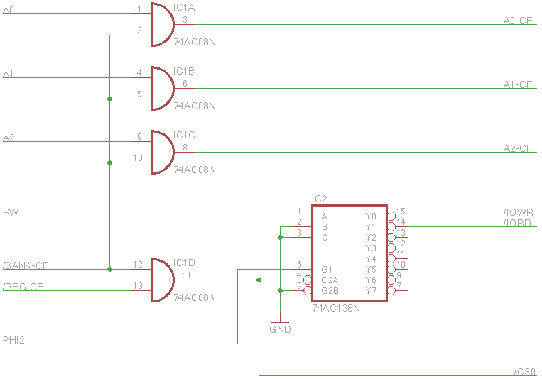
/REG-CF is the normal select signal to access the registers of the IDE Task File and is only asserted (low) when you normally access the registers in PIO mode. The /BANK-CF is asserted whenever you want to access the DATA Register. /BANK-CF is asserted for one entire bank, but due to the AND gates whatever address within the bank is accessed it always selects the Data register of the Task File. So you can use the MVN or MVP instructions to transfer the sector buffer to/from memory.
As for busses in Eagle I used them, but only for signals with suffixes, so I named the Bus like A[0..15]. But did not know you can specify a free list of signal names, separated with comma, and even mix and match both, signals with suffixes and individual names in one bus. That's really a cool feature. Then together with the labels it makes even a complex schematic neat and clean. Thanks for the hint.
I did not find the time to redraw all signals and busses using your trick. But nevertheless, so you don't have to wait too long, here the preliminary drawings of my design
First the core with the CPU, Memory, Keyboard, DP-RAM (Video), Clock and Reset circuit
 Viewed 2277 times")
- SBBC Main Parts
As next follows decoder, the internal IO required to emulate the Apple II and other logic packed into GALs
 Viewed 2277 times")
- SBBC Internal IO
And the last drawing contains the IO connected to the IO Extension slot
 Viewed 2277 times")
- SBBC External IO (IO Expansion Bus)
The two SC2691 (UART) are not drawn yet, but are not required to get an idea of my design. I use GALs instead of a CPLD (I have not yet jumped into this cold water) and as it is at the moment they are used very inefficiently. You could achieve the same result with just 3 GALs. This is mainly because I built the SBBC step by step before I had the final design and made many design changes during the soldering sessions. However it does have all the features I wanted it to have from the beginning. These were PS/2 Keyboard, VGA Display and a mode that emulates an Apple IIe. E.g. I never wanted to decode the full 16Mbyte address space (I need only 512kbyte RAM). Even better, instead of a real 16-bit IDE I use the CF-Cards in 8-bit IDE mode which made the interface a piece of cake.
Regards
Peter
Re: SBC Blaufuchs-II
Posted: Fri Jun 27, 2014 7:00 pm
by BigDumbDinosaur
— BUMP —
Wonder if norby got this built and if so, if it's up and running.
Re: SBC Blaufuchs-II
Posted: Sun Aug 17, 2014 11:04 am
by norby
No not yet.
All components has been sourced.
First draft of the CPLD code has been done and somewhat tested.
PCB design is done.
Then the summer hit!
I will pick up where I left when the wheater turns cold ... which is starting to happen now...
/norby
Re: SBC Blaufuchs-II
Posted: Mon Aug 18, 2014 8:12 pm
by cbscpe
At least your summer was a hit, in Switzerland it was 6 weeks of continuous rain. I managed to spend just 2 days at the pool these weeks.
Re: SBC Blaufuchs-II
Posted: Sun Aug 07, 2016 7:59 am
by BigDumbDinosaur
-- BUMP --
Whatever happened with Norby's project?