Page 3 of 4
Re: Design of NEW 3.3V Devboard 'Backplane'
Posted: Sun Oct 28, 2012 2:27 am
by GARTHWILSON
I post v1.0d at the head because I have a preliminary final design.
I'm not sure I understand. I see "v1.0a" and "v1.0b" on the board images, but no "v1.0d", and the image above has some design-rules violations, primarily the green trace from pin 14 of the control slot going too close to a via for another net, and another thing about the same right near pin 74 of PVB3.
Re: Design of NEW 3.3V Devboard 'Backplane'
Posted: Sun Oct 28, 2012 10:46 am
by ElEctric_EyE
I'm not sure I understand. I see "v1.0a" and "v1.0b" on the board images, but no "v1.0d"...
Version 1.0b is what I meant, sorry about that. Version 1.0a is flawed, that design was just before I made major modifications based on your advice and it was right after I had realized I was erroneously still using the 4 layer board option. At least you haven't found errors on v1.0b. I'm still looking myself, and I hopefully can get to updating the head post about pin assignments today.
Re: Design of NEW 3.3V Devboard 'Backplane'
Posted: Sun Oct 28, 2012 11:24 pm
by ElEctric_EyE
Work was busy, so I could not do the pin assignments which requires much dedicated 'uninterrupted' time. But I did find an error on the layout, and optimized some routings. Header should be updated soon.
On a side note, I received parts from Digikey for a few 'pass-thru' PVB's using minimal parts. These pass-thru PVB's would potentially be PVB1 thru PVB5... I should spec one of these boards on the PVB thread... I'll be able to catch up Tue&Wed.
Re: K1 Controller board Pin Assignments
Posted: Mon Oct 29, 2012 6:56 pm
by ElEctric_EyE
Ok, finished the pin assignments for the controller board. Following the traces for each pin led me to one more shorted signal on PVB1. This I believe to be the last error, and the head pic has been updated. I have the funds needed for a board run and will make one tomorrow if nothing else comes up...
Re: Design of NEW 3.3V Devboard 'Backplane'
Posted: Mon Oct 29, 2012 7:02 pm
by GARTHWILSON
There appear to be traces touching pads they shouldn't at pins 17 and 50 of the connectors, but I realize that what I'm seeing might just be round-off errors in the drawing for the small size. Be sure to visually scan both layers individually, blown way up, up and down the rows.
Re: Design of NEW 3.3V Devboard 'Backplane'
Posted: Mon Oct 29, 2012 7:33 pm
by ElEctric_EyE
Good eye Garth, they're shorted but
pins 17 & 50 are GND on each PVB.
Re: Design of NEW 3.3V Devboard 'Backplane'
Posted: Mon Oct 29, 2012 7:38 pm
by BigEd
This looks wrong to me:
- drc.png (20.56 KiB) Viewed 1850 times
Do you have a DRC checker?
Cheers
Ed
Re: Design of NEW 3.3V Devboard 'Backplane'
Posted: Mon Oct 29, 2012 7:47 pm
by GARTHWILSON
If they're supposed to make contact, I would recommend making the trace head directly into to the pad, so there aren't angles of much under 90° in the copper. My understanding from one of our PCB supplierss' explanation is that it makes it harder for them to get a good yield of reliable boards. Ed's picture shows what could turn out to be a problem. BTW, there's nothing wrong with straying from 0-45-90° trace angles. Make them whatever you need to.
Re: Design of NEW 3.3V Devboard 'Backplane'
Posted: Mon Oct 29, 2012 7:52 pm
by ElEctric_EyE
Well, I've tried to keep the GND's in parallel with the high speed clock signal pretty much equidistant, even around bends... EDIT: I will enlarge the copper even more for the types in BigEd's snapshot.
Re: Design of NEW 3.3V Devboard 'Backplane'
Posted: Mon Oct 29, 2012 8:46 pm
by GARTHWILSON
If your CAD doesn't have teardropping, you can zoom way in and add little traces in the corners to accomplish the same purpose. Keeping "equidistant" keeps a consistent transmission-line characteristic impedance (if other things remain equal too), but that in itself is probably pretty meaningless if you're not keeping to a particular value and terminating to that value. You'll still be keeping the signal's return current very closeby which accomplishes much of the desired goal.
Re: Design of NEW 3.3V Devboard 'Backplane'
Posted: Mon Oct 29, 2012 9:55 pm
by ElEctric_EyE
Thanks Garth & Ed, I think I may have something worthy of manufacture now. Maybe this one will be without 1 mistake. Updated header pic. I'll be able to polish off the rest of the header tonight when I get home.
Re: Design of NEW 3.3V Devboard 'Backplane'
Posted: Tue Oct 30, 2012 2:16 pm
by ElEctric_EyE
Updated...
Time to move on! I'm rolling the dice with this final version. It's in the queue...
Re: Design of NEW 3.3V Devboard 'Backplane'
Posted: Tue Nov 06, 2012 10:33 pm
by ElEctric_EyE
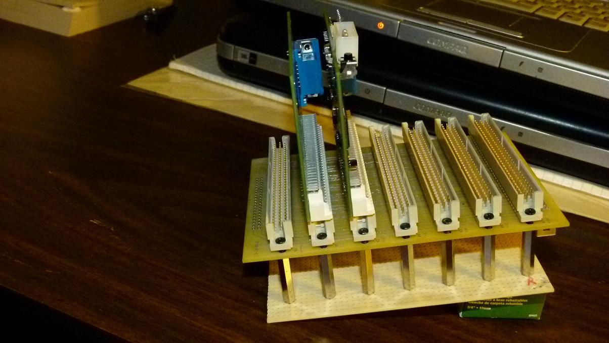
I just received the boards. Tomorrow, I will solder in the receptacles and put together 1 PVB bypass board. Will document how to do this on that thread.
Re: Design of NEW 3.3V Devboard 'Backplane'
Posted: Wed Nov 07, 2012 2:33 pm
by ElEctric_EyE
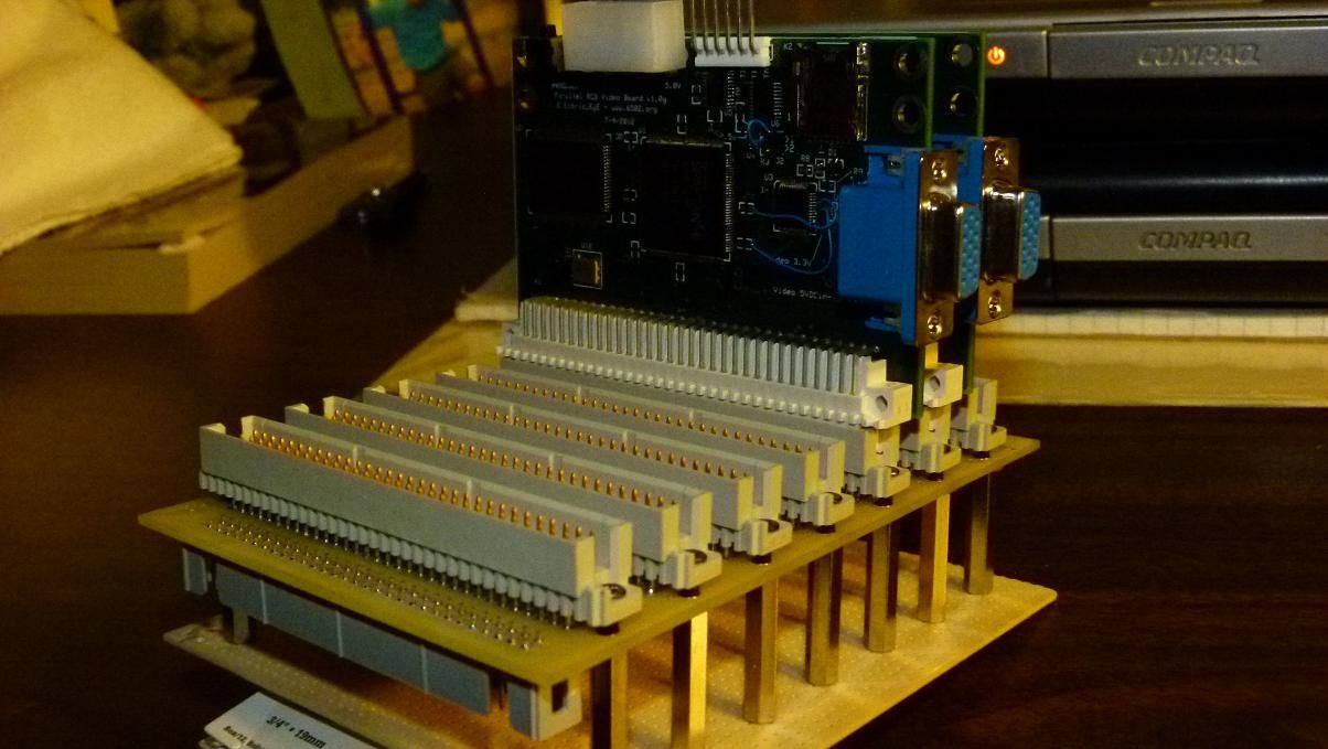
I'm done soldering today. 800+ holes. Will do another PVB board next week.
More form than function at this point...
Re: Design of NEW 3.3V Devboard 'Backplane'
Posted: Wed Nov 07, 2012 4:16 pm
by BigDumbDinosaur
I'm done soldering today. 800+ holes. Will do another PVB board next week.
More form than function at this point...
Sounds like an excuse to devise a wave-soldering station!  Them there's a lot of holes.