Page 3 of 15
Re: Breaking 6502 apart
Posted: Sat Jul 07, 2012 6:29 pm
by org
Todays speccy : Program Counter Low part (PCL)
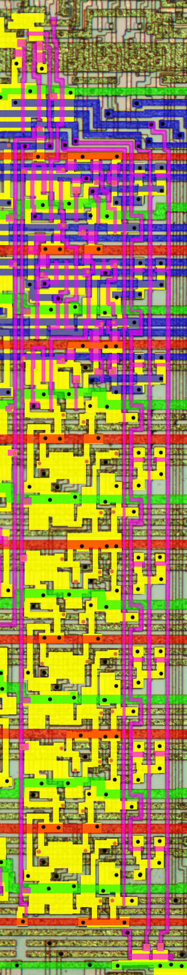
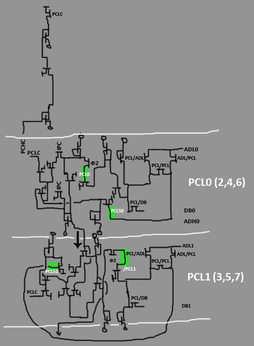
I do not know (yet) why these regular structures are different between PCL0/2/4/6 and PCL1/3/5/7.
Also PCL1/3/5/7 saved in latch in inverted form.
Input driver signal is IPC (increment PC).
Output goes from PCLn latch and optionally feed back to PCLSn latch, if PCL/PCL is driven high.
Re: Breaking 6502 apart
Posted: Sat Jul 07, 2012 10:35 pm
by Dr Jefyll
I do not know (yet) why these regular structures are different between PCL0/2/4/6 and PCL1/3/5/7.
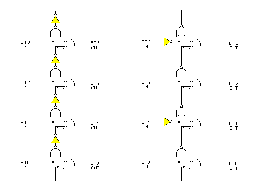
The difference is due to inverters in the path of alternate data bits (eg: PCL1/3/5/7). This is part of a logic optimization that results in a faster incrementer. The incrementer's most critical path is not the individual data bits but the Carry chain that cascades from one stage to the next -- a total of 8 levels. In order to build the fastest incrementer, all efforts must focus on speeding up the Carry chain. To this end it proves advantageous to operate each alternate incrementer stage with active-low logic (where logic
low represents a
1). That means
adding inverters around the incrementer stage of each alternate data bit, but it effectively allows the
elimination of eight inverters from the Carry chain. (I'll try to rustle up a diagram illustrating this.)
-- Jeff
edit: "allows the elimination of
eight inverters from the Carry chain" (not four)
Re: Breaking 6502 apart
Posted: Sun Jul 08, 2012 7:56 am
by org
Thanks for explanation Jeff, I understood - this trick is need to reduce propagation delay.
Re: Breaking 6502 apart
Posted: Sun Jul 08, 2012 4:31 pm
by Dr Jefyll
Thanks for explanation Jeff, I understood - this trick is need to reduce propagation delay.
To reduce propagation delay, yes. In case anyone else is wondering, here's the diagram -- which hopefully is an improvement over my verbal description! The diagram shows the incrementer (just the first four stages) before and after optimization. The optimized version (on the right) uses active-low logic in alternate stages. (I've drawn bits 1/3/5/7 as being the ones that are inverted but in fact it may be bits 0/2/4/6 instead; I don't know.)
The two versions produce identical results, but the unoptimized version is slower because it's obliged to employ inverters in the Carry path. That's because an AND function is required, which must be implemented as NAND followed by an inverter. Of course the optimized version also features inverters, but they don't result in a cumulative delay because they're not part of the eight-level Carry chain.
- incrementer stages .gif (7.19 KiB) Viewed 2522 times
Edit: alteration to diagram (see subsequent posts)
Re: Breaking 6502 apart
Posted: Sun Jul 08, 2012 6:38 pm
by org
Thanks for the drawings, you saved a lot time for me )
Meanwhile, todays speccy : Program Counter High part (PCH)
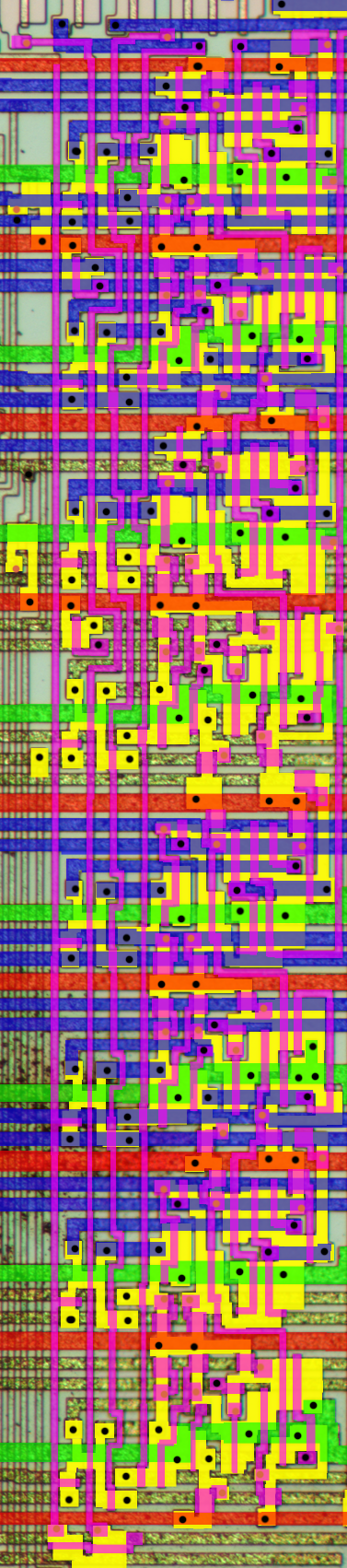
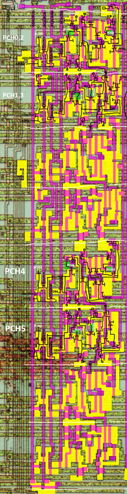
Nothing unusual here ) Same optimized incrementer, but there is separated increment logic for PCH0-3 and PCH-4-7.
PCH0-3 feeds PCLC and output PCHC, which is routed to PCH4-7.
Both schematics perfectly fit in D.Hanson diagram :
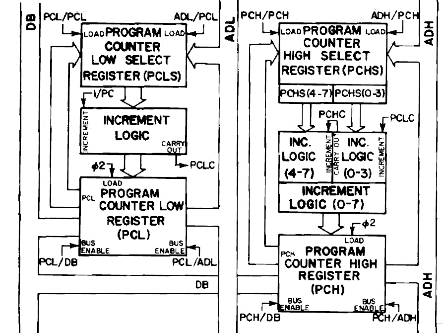
Code: Select all
PHI1:
if (PCL/PCL) PCLS = PCL;
if (ADL/PCL) PCLS = ADL;
if (PCL/PCL && ADL/PCL) PCLS = PCL & ADL;
if (PCH/PCH) PCHS = PCH;
if (ADH/PCH) PCHS = ADH;
if (PCH/PCH && ADH/PCH) PCHS = PCH & ADH;

if (IPC) PCLS++;
if (PCLS == 0) PCHS++;

if (PCL/DB) DB = PCL;
if (PCL/ADL) ADL = PCL;
if (PCH/DB) DB = PCH;
if (PCH/ADH) ADH = PCH;

PHI2:
PCL = PCLS;
PCH = PCHS;
ADH = ADL = DB = 0xFF
Re: Breaking 6502 apart
Posted: Sun Jul 08, 2012 9:09 pm
by leeeeee
Do you need to invert every other output bit?
Inverting both inputs to an exclusive OR gate leaves the output unchanged.
Lee.
Re: Breaking 6502 apart
Posted: Sun Jul 08, 2012 10:10 pm
by Dr Jefyll
D'oh! You're right. In negative logic the XOR function is accomplished by an XNOR gate. So for bits 1,3,5,7 I should've drawn XNOR... followed by an inverter because the output is supposed to drive circuitry using positive logic. Of course XNOR followed by an inverter is the same as simply XOR. I'll fix the diagram. Thanks, Lee.
-- Jeff
Re: Breaking 6502 apart
Posted: Mon Jul 09, 2012 7:33 am
by BigEd
Found
one of my old posts which points us to
this page by Dieter Mueller.
Re: Breaking 6502 apart
Posted: Mon Jul 09, 2012 8:46 am
by GARTHWILSON
Dieter has updates coming too.
Re: Breaking 6502 apart
Posted: Mon Jul 09, 2012 2:21 pm
by org
More progress on crazy logic :
Image no longer available: http://ogamespec.com/imgstore/whc4ffae6ac6ec5a.jpg
I began to understand how it works in general

PLA outputs are joined in "groups".
Groups on the left works with X,Y and S registers (resided underneath).
Groups on the middle are ALU related, which feed its inputs.
Groups on the right are branch/flag/compare and (possibly) interrupt/reset logic; instructions related to program counter (PC is resided on the bottom right side of the 6502).
Also there is intense metall layer crosspassing from the left to the right, for addressing calculations purposes.
Hope to crunch it fast, when I get full color schematics (good for LSD trips BTW

)
Re: Breaking 6502 apart
Posted: Mon Jul 09, 2012 5:05 pm
by org
In case someone interested, Visual6502 wiki has hidden section, which I found by poking Random page:
http://visual6502.org/wiki/index.php?ti ... atic_Notes
There is poor photos of 6502 blueprints.
Re: Breaking 6502 apart
Posted: Tue Jul 10, 2012 1:14 pm
by Unseen
There is poor photos of 6502 blueprints.
Actually it's not a photo but a size-reduced version of a scan of the blueprint. A photo would have no or different artifacts at the places where overlapping sections are merged.
Re: Breaking 6502 apart
Posted: Wed Jul 11, 2012 6:04 am
by org
I mean images ) Sorry my language )
Re: Breaking 6502 apart
Posted: Wed Jul 11, 2012 1:02 pm
by org
Todays speccy: Random logic A/B groups.
I separated PLA outputs on groups A,B,C,D,E,F,G,H and K.
Here is preview of below schematics :
Image no longer available: http://ogamespec.com/imgstore/whc4ffd765f41d7c.jpg
Top part:
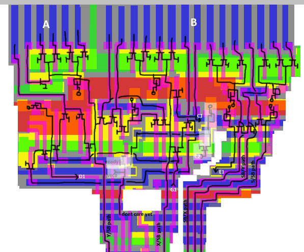
Bottom part:
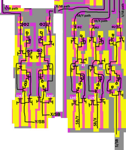
Also there is small logic to generate internal 43 and 1247 lines, which are used on bottom part:
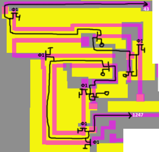
(I do not understand wtf is it... some kind of /Ф1 power-up?)
I labeled interconnections between groups by white text.
Re: Breaking 6502 apart
Posted: Wed Jul 11, 2012 7:19 pm
by org
More progress on ALU:
Image no longer available: http://ogamespec.com/imgstore/whc4ffdd1751cca0.jpg