Added: at some point we also discussed a micro SD card holder. This is also a fast way to get access to huge amounts of user data. The only disadvantage is that accessing the data from the FPGA requires a lot more software support.
Future plans for Dev. Board v1.2
Re: Future plans for Dev. Board v1.2
ElEctric_EyE wrote:
I was planning on using the SPI serial FLASH as data/program storage not for FPGA boot.
Added: at some point we also discussed a micro SD card holder. This is also a fast way to get access to huge amounts of user data. The only disadvantage is that accessing the data from the FPGA requires a lot more software support.
-
ElEctric_EyE
- Posts: 3260
- Joined: 02 Mar 2009
- Location: OH, USA
Re: Future plans for Dev. Board v1.2
Arlet wrote:
...Added: at some point we also discussed a micro SD card holder. This is also a fast way to get access to huge amounts of user data. The only disadvantage is that accessing the data from the FPGA requires a lot more software support.
Yes, the software. Even though I try to make this board relatively simple, there are things which will take time to develop.
On the note of having 2 config PROMs and 2 large serial FLASHs. It should make it easier to keep track of what's going on for each config even if some data is redundant. One config could use 1 FLASH and the other config could use the other. Just one of the possibilies...
-
ElEctric_EyE
- Posts: 3260
- Joined: 02 Mar 2009
- Location: OH, USA
Re: Future plans for Dev. Board v1.2
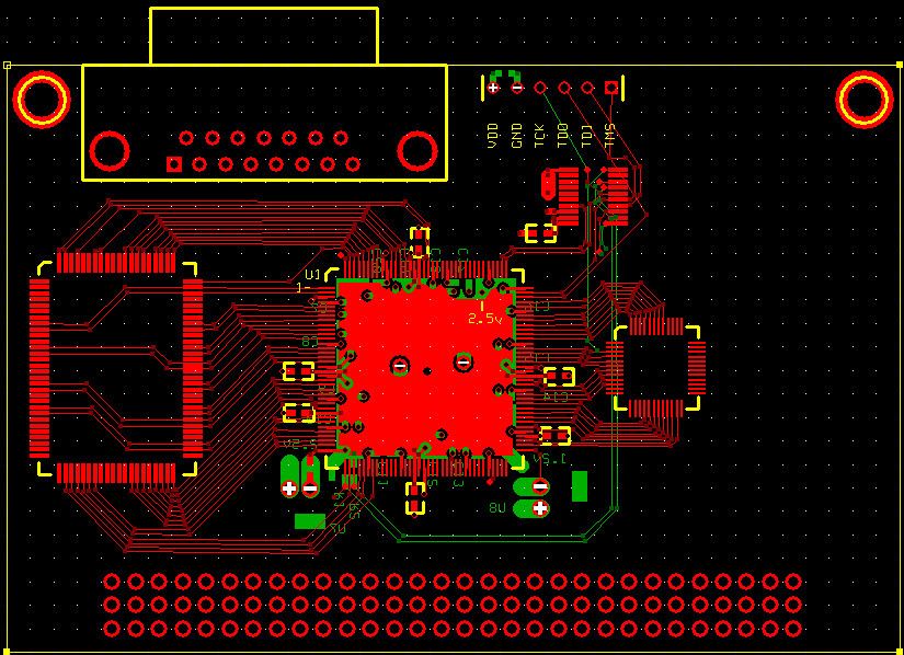
Super slow at work today, so I got around to general placement of the main IC's: RAM, FPGA, and video DAC. FPGA Proms/JTAG still need attention. But I'm already about half way done I would say. Came out very nice and tight first time around. Looks like there'll be enough space for all IC's to be on top of the board. So far 33 pins to spare on the FPGA.
Earlier I had wanted for the Master board to be able to peer into the video ram and this could've been done with another CPLD to MUX the address and data buses, but it also would have added close to 10ns delay, which for high speed video could not be tolerated. And thus I have a big honkin connector. Originally I had wanted the connector to be standard on all boards, but I am rethinking this.
I must come up with a system of communication from an outside controlling board to this board. I'm thinking of some simple X, Y 16-bit registers and a command register for plotting pixels, shapes, etc.

Re: Future plans for Dev. Board v1.2
How do you solder the surface mount parts? How is that done?
- GARTHWILSON
- Forum Moderator
- Posts: 8773
- Joined: 30 Aug 2002
- Location: Southern California
- Contact:
Re: Future plans for Dev. Board v1.2
answered in this topic: viewtopic.php?f=4&t=1492
http://WilsonMinesCo.com/ lots of 6502 resources
The "second front page" is http://wilsonminesco.com/links.html .
What's an additional VIA among friends, anyhow?
The "second front page" is http://wilsonminesco.com/links.html .
What's an additional VIA among friends, anyhow?
-
ElEctric_EyE
- Posts: 3260
- Joined: 02 Mar 2009
- Location: OH, USA
Re: Future plans for Dev. Board v1.2
whartung wrote:
How do you solder the surface mount parts? How is that done?
-
ElEctric_EyE
- Posts: 3260
- Joined: 02 Mar 2009
- Location: OH, USA
Re: Future plans for Dev. Board v1.2
Anyone know how difficult it would be to mix or overlay 2 or more VGA images, either digitally or after the DACs?. Same resolutions and HSYNC VSYNC.
Difficult to find info. I'm currently looking for ICs that may perform this function.
EDIT: To do it digitally, is it as simple as XORing the RGB digital before the DACs?
Difficult to find info. I'm currently looking for ICs that may perform this function.
EDIT: To do it digitally, is it as simple as XORing the RGB digital before the DACs?
-
ElEctric_EyE
- Posts: 3260
- Joined: 02 Mar 2009
- Location: OH, USA
Re: Future plans for Dev. Board v1.2
Thinking about it more, it's probably not a good idea to do it digitally as there will be a delay affect as each board is cascaded. I need something like a summation of each board's R,G and B after the DAC. I wonder if a simple resistor divider network will work?
-
ElEctric_EyE
- Posts: 3260
- Joined: 02 Mar 2009
- Location: OH, USA
Re: Future plans for Dev. Board v1.2
Resistor divider won't work either. If one board had a blue propeller spinning clockwise and another board had a red propeller spinning counter-clockwise, where the propellers intersected would be purple, which is not going to work. I need a layer type of organization with a priority for each board. May be too difficult. Will have to think about it further...
My idea would've worked for a monochrome system though.
Re: Future plans for Dev. Board v1.2
I think digital is best, especially as you have a whole FPGA to play with.
You can always delay the local strea to match the remote stream as you cascade things.
Cheers
Ed
You can always delay the local strea to match the remote stream as you cascade things.
Cheers
Ed
-
ElEctric_EyE
- Posts: 3260
- Joined: 02 Mar 2009
- Location: OH, USA
Re: Future plans for Dev. Board v1.2
Yes, I think you're right. We can use notation in Verilog to set a delay. I've never played around with this and don't know how precise it is, but it can't hurt to try. Plus there might be some neat effects from the delay during experimentation... I wonder what the bottleneck will be for the number of boards running in "parallel"? or is it serial?
Quickly running out of pins on the FPGA. 24 more for RGB in, leaves just 8.
So now the 96-pin main header begins to fill up:
16 pins for databus
24 pins for RGB in
24 pins for RGB out
64 pins used + some extraneous clock/control signals.
Now I must rearrange how the RAM is connected to the FPGA to make room for RGB in.
Re: Future plans for Dev. Board v1.2
ElEctric_EyE wrote:
Yes, I think you're right. We can use notation in Verilog to set a delay.
-
ElEctric_EyE
- Posts: 3260
- Joined: 02 Mar 2009
- Location: OH, USA
Re: Future plans for Dev. Board v1.2
Arlet wrote:
The verilog delay notation is not synthesizable. In hardware, you can delay a signal by using flip-flops, fifo, or shift registers by a whole number of clock cycles.
My plans today are to refresh my memory with UG393, I/O pin planning, and make progress with finalizing the layout quickly in order to determine how many pins I'll have for control communications. Unfortunately, I'm thinking that it's going to be serial with the lack of necessary pins for any kind of parallel.
Re: Future plans for Dev. Board v1.2
Mixing digital VGA images should be fairly simple if you cascade the boards, and make sure you supply the pixel clock with the RGB signal.
-
ElEctric_EyE
- Posts: 3260
- Joined: 02 Mar 2009
- Location: OH, USA
Re: Future plans for Dev. Board v1.2
Glad you're confident about the concept! Those signals will be present.
No promises but with so much space left on the back of the board I am looking into adding HDMI 1.4 with a 100-pin QFP ADV7511. The video portion looks easy, although the I2C control signals may have to come from offboard, maybe the future soundboard since HDMI makes provisions for I2S audio. There's room for these signals on the main connector. More research is necessary...