Page 3 of 7
65Org16 is open sourced
Posted: Mon May 16, 2011 7:46 pm
by BigEd
With some help from Arlet, I've put my sources
into place on github - they are LGPL licensed which basically means "open-sourced but if you distribute any designs you also need to distribute the sources". (So any fixes or enhancements should stay out in the open)
The main branch in this project is Arlet's 6502-compatible core. I've staked out a branch called 65Org16-master for my core. As usual with github, take a fork if you'd like to join in the development, or download the source and have a play. (There's a big Downloads button - you can't miss it!)
I hope to add the (simple) assembler shortly.
There's still no RAM in the system-on-FPGA - I didn't get around to doing that today.
Cheers
Ed
Re: 65Org16 is open sourced
Posted: Tue May 17, 2011 10:10 pm
by ElEctric_EyE
With some help from Arlet,...
Cheers
Ed
I was wondering if Arlet was for or against you modding his core. That's nice to know he is actually helping.
I really do wish I had time to experiment with this! Maybe soon...
Posted: Fri May 20, 2011 12:31 am
by ElEctric_EyE
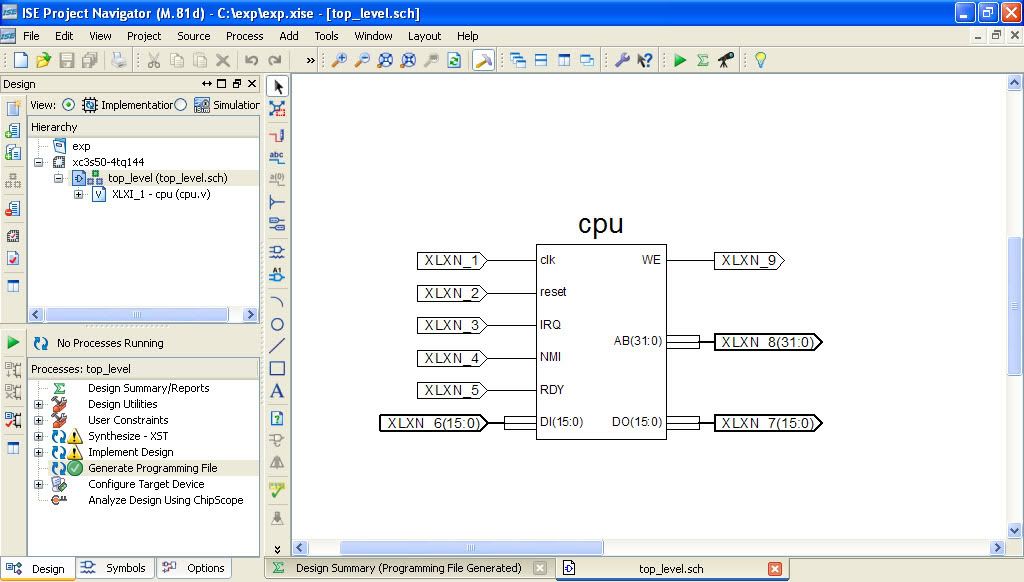
Ok, now I've got a few hours to spare and have downloaded the files, and put them through ISE synth (I'm sure you guys have too). I tried first to fit the 65ORG16 core into the smallest FPGA Xilinx has to offer that can hold RAM & ROM, i.e. the smallest of the Spartan 3 series, the XC3S50 in 100-pin QFP. It did not fit, I think only because it didn't have enough pins. However, it did fit into the XC3S50 144-pin QFP package and here are the passing synthesis results for the core only:
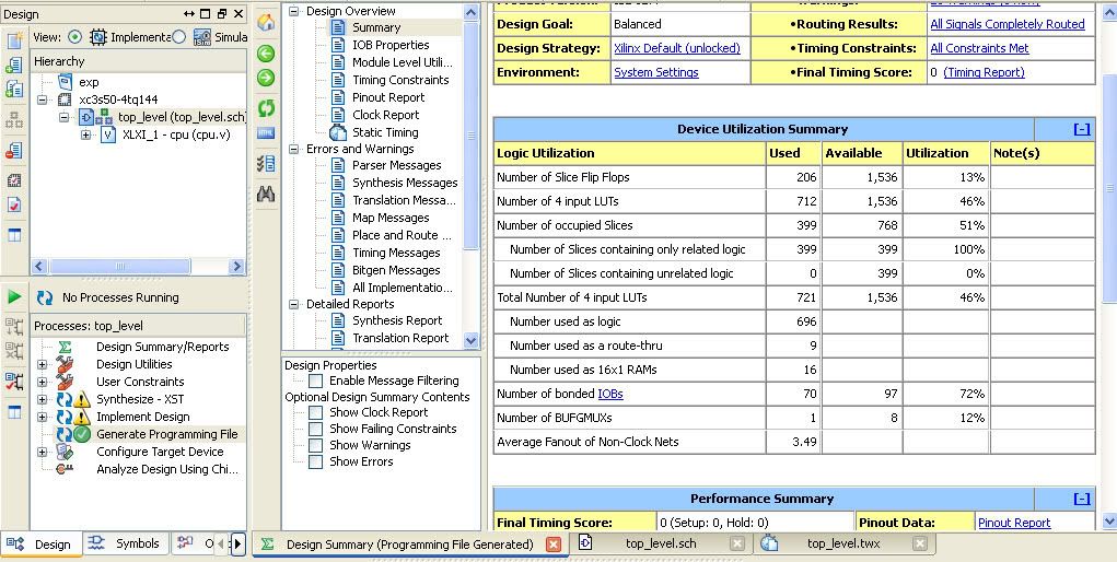
Also, here is the pinout:
I'll tell you what, a while ago I would've considered the MC68000 for a
true 16-bit CPU... This 65ORG16 is now on my top shelf for experimentation when it comes to a cpu with a true 16-bit databus...
Posted: Fri May 20, 2011 8:39 am
by Arlet
I've programmed on the 68000, and even though it has a nice architecture with plenty of registers and instruction modes, the instruction timing isn't too impressive. A simple move from one register to another already takes 4 cycles, and the more complex 32 bit moves can take over 30 cycles.
Posted: Fri May 20, 2011 11:58 am
by ElEctric_EyE
So I would guess the timing for the 65ORG16 core is identical to the original?
Only problem is I wouldn't be able to develop on it, by using it alone, like what I'm attempting to do on the 6502SoC. So much software has been already made for the 6502 and the 68000... However, that isn't such a problem that it would stop me from developing with it. Just waiting for the assembler so I can tinker...

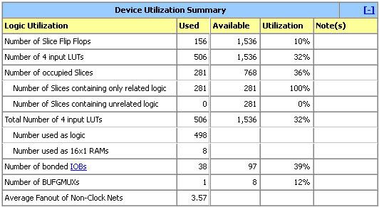
Here's the synthesis results for Arlet's 8-bit original just for comparison...
If I were going to maximize the 144-pin package, I would use the
Spartan 3 XC3S400 or the
Spartan 6 XC6SLX9.
Posted: Fri May 20, 2011 12:02 pm
by Arlet
I'm expecting the 16 bit version to be somewhat slower, but if you take out the BCD code (which doesn't work properly in 16 bit mode anyway), the difference should be minimal (16 bit without BCD might even be faster than 8 bit with BCD).
(The problem with the BCD mode is that it is only applied to the bottom 8 bits)
Posted: Fri May 20, 2011 12:16 pm
by BigEd
EE:
Yes, the cycle timings are the same, although as Arlet says the clock speed will vary,
I'm hoping for a license update on Dave Beazley's assembler so I can include that in the project - but I should warn you it is basic and non-standard. It is certainly good enough for small test programs, a bootstrap loader, maybe a monitor. It would be fine as the back end to a compiler. But for general use we might need something else: almost certainly it would be best to port an existing 6502 assembler.
If anyone is interested in doing that, it would be good to talk!
(There's also no harm in having more than one. Personally, I need to stay focussed on the hardware side for now: I want to have a development platform with a program loader.)
Posted: Fri May 20, 2011 12:19 pm
by Arlet
Ed, have you already used the RDY input ?
Posted: Fri May 20, 2011 12:21 pm
by BigEd
(The problem with the BCD mode is that it is only applied to the bottom 8 bits)
Yes, I know. I should at least add a comment to this effect! My current official position is that it is undefined, which means I can remove it when I get around to it.
Posted: Fri May 20, 2011 12:23 pm
by BigEd
Ed, have you already used the RDY input ?
Not yet. (were you planning a change?)
My idea is to connect the external SRAM I have - it's slow, and only 8 bits wide, so at minimum I'll need a buffer and in due course I'd like to build a cache. In both cases, RDY will be useful.
Cheers
Ed
Posted: Fri May 20, 2011 12:30 pm
by Arlet
No, I wasn't planning a change. I was just wondering if everything was working correctly. It would be nice to see it working properly with external memories.
Posted: Fri May 20, 2011 4:41 pm
by BigEd
Hi Arlet, agreed, that will be a good point to get to, and I hope to get there.
At the moment I'm struggling with the block rams. I have them working - in simulation - but only by clocking on the wrong edge. I haven't got the hang of the clocking of the core.
Looking at the detailed post-routing timing reports, I see:
- clock to clock meets 20ns period
clock to output (address bus) is 25ns
input to clock (data in) is 20ns
input to output (data in to address bus) is 20ns
That's quite a big combinatorial path inside the CPU. Have you a block diagram sketch of where (in timing boundary terms) the CPU and the external memory relate to one another?
(It seems that the data in arrives really early, and the address bus leaves really late.)
Posted: Fri May 20, 2011 4:53 pm
by GARTHWILSON
I'm expecting the 16-bit version to be somewhat slower, but if you take out the BCD code (which doesn't work properly in 16-bit mode anyway), the difference should be minimal (16-bit without BCD might even be faster than 8-bit with BCD).
(The problem with the BCD mode is that it is only applied to the bottom 8 bits)
BCD is applied to 4 bits at a time, and will work fine with any multiple of 4 bits. (I'm not saying it's essential though, as I haven't used it in decades myself.)
Posted: Fri May 20, 2011 4:55 pm
by Arlet
My memory attachment looks like this:
Code: Select all
ram ram( .clk(clk),
         .AB(AB),
         .DO(DI_RAM),
         .DI(DO),
         .WE(WE),
         .vclk(vmem_clk),
         .VAB(vmem_addr),
         .VDO(vmem_data)
);

boot boot( .clk(clk),
         .AB(AB),
         .DO(DI_OS),
         .DI(DO),
         .WE(WE)
);


assign DI = DI_OS | DI_RAM;

cpu cpu( .clk(clk),
         .reset(reset),
         .AB(AB),
         .DI(DI),
         .DO(DO),
         .WE(WE),
         .IRQ(1'b0),
         .NMI(1'b0) );
And the ram is implemented like this:
Code: Select all
wire sel_0000 = (AB[15:10] == 6'b0000_00);
wire sel_8000 = (AB[15:10] == 6'b1000_00);

wire EN = (sel_0000 | sel_8000);

RAMB16_S9_S9 ram_0000_03ff_and_8000_83ff(
        .CLKA( clk ),
        .WEA( WE & EN ),
        .ENA( 1'b1 ),
        .SSRA( ~EN ),
        .ADDRA( {AB[15], AB[9:0]} ),
        .DOA( DO ),
        .DIA( DI ),
        .DIPA( 0 ),

        .CLKB( vclk ),
        .WEB( 1'b0 ),
        .ENB( 1'b1 ),
        .SSRB( 1'b0 ),
        .ADDRB( {1'b1, VAB[9:0]} ),
        .DOB( VDO )
);
Did you include flip flops on the outputs of the external memories ? They are supposed to be registered, otherwise you can never get decent timing.
Then you'll have a long combinatorial path from the memory data output to the DI port, and through the ALU. Of course, you can cut this path in two by also registering the inputs, but then you'll need to use RDY.
Posted: Fri May 20, 2011 4:58 pm
by Arlet
BCD is applied to 4 bits at a time, and will work fine with any multiple of 4 bits. (I'm not saying it's essential though, as I haven't used it in decades myself.)
Sure, but in Ed's code, he just copied my 8-bit BCD code, and widened the data bus to 16 bits, without adding another BCD stage for the MSB.