Completley forget about doing any internal logic with signals with multiple drivers.
FPGAs do not work like that. In fact, modern CMOS does not work like that. If you ask for a multi-driver bus, then the software will synthesize it poorly by building a big multiplexer somewhere for all your outputs, then feeding all the inputs off the output of the mux.
The bus that connects to the outside world can go as input to all your components; thats fine. Now, build a mux, and feed it the outputs of all your devices. However you want the mux to work is up to you; it can either be just an OR of them all (and they each have their own shutoffs), or it can be an actual selector fed with the address decode logic. The output drivers of this mux should be controlled by the read/write signal.
Because you're now designing to the hardware, you'll find things work better. They will also be smaller.
(This is one of the reasons I recommend anyone planning on doing FPGA/CPLD work learn Verilog or VHDL. They make you think much more closely about how the hardware actually works. In the long run, you will also find it much faster to work in.)
Getting started with Xilinx CPLD's & FPGA's
-
ElEctric_EyE
- Posts: 3260
- Joined: 02 Mar 2009
- Location: OH, USA
@OwenS,
It is nice to finally be able to post here in the 6502 forums as a beginner to CPLD/FPGA design and have someone familiar, with more knowledge offer a more expert advice! I post in the Xilinx forums rarely because I am a proponent of schematic design... I seem to be the only one!
A multiple driver design 'error' implies a design with feedback, thus inputs and outputs are in conflict. Xilinx CPLD's seem to give you more room in this regard. More room than their FPGA's.
How would a FPGA design correctly implement multiple internal I/O ports through a single external bus?

ElEctric_EyE wrote:
How would a FPGA design correctly implement multiple internal I/O ports through a single external bus?
Defenition of the data bus and the use of it:
Code: Select all
entity RB65 is
  Port (
    ......
    D		: inout	std_logic_vector(7 downto 0);
    ......
  );
end RB65;

architecture AR_RB65 of RB65 is

  D <= std_logic_vector(D_out) when ((PHI_i = '1') and (RW_i = '0'))
        else "ZZZZZZZZ";

  IntData <= unsigned(D) when (PHI0 = '1');	-- read data
  Opcode <= unsigned(D) when ((PHI0 = '1') and (OpcC_Reset = '1'));
  SYNC <= '1' when ((PHI_0 = '1') and (OpcC_Reset = '1')) else '0';

end AR_RB65;
IntData holds the data read at every clock, Opcode speaks for itself IMHO.
Have fun!
Last edited by Ruud on Fri Oct 22, 2010 6:21 am, edited 1 time in total.
Code: Select all
    ___
   / __|__
  / /  |_/     Groetjes, Ruud
  \ \__|_\
   \___|       URL: www.baltissen.org
-
BigDumbDinosaur

- Posts: 9428
- Joined: 28 May 2009
- Location: Midwestern USA (JB Pritzker’s dystopia)
- Contact:
Code: Select all
entity RB65 is
Port (
......
D : inout std_logic_vector(7 downto 0);
......
);
end RB65;

architecture AR_RB65 of RB65 is

D <= std_logic_vector(D_out) when ((PHI_i = '1') and (RW_i = '0'))
else "ZZZZZZZZ";

IntData <= unsigned(D) when (PHI0 = '1'); -- read data
Opcode <= unsigned(D) when ((PHI0 = '1') and (OpcC_Reset = '1'));
SYNC <= '1' when ((PHI_0 = '1') and (OpcC_Reset = '1')) else '0';

end AR_RB65; x86? We ain't got no x86. We don't NEED no stinking x86!
BigDumbDinosaur wrote:
A more readable version of his VHDL.
Code: Select all
    ___
   / __|__
  / /  |_/     Groetjes, Ruud
  \ \__|_\
   \___|       URL: www.baltissen.org
-
ElEctric_EyE
- Posts: 3260
- Joined: 02 Mar 2009
- Location: OH, USA
ElEctric_EyE wrote:
...How would a FPGA design correctly implement multiple internal I/O ports through a single external bus?
I post for us beginners.
-
ElEctric_EyE
- Posts: 3260
- Joined: 02 Mar 2009
- Location: OH, USA
BigDumbDinosaur wrote:
Code: Select all
entity RB65 is
Port (
......
D : inout std_logic_vector(7 downto 0);
......
);
end RB65;

architecture AR_RB65 of RB65 is

D <= std_logic_vector(D_out) when ((PHI_i = '1') and (RW_i = '0'))
else "ZZZZZZZZ";

IntData <= unsigned(D) when (PHI0 = '1'); -- read data
Opcode <= unsigned(D) when ((PHI0 = '1') and (OpcC_Reset = '1'));
SYNC <= '1' when ((PHI_0 = '1') and (OpcC_Reset = '1')) else '0';

end AR_RB65; Might have been an error in my code though.
Is there a specific difference between CPLDs and FPGAs in that respect?
Thanks
André
Hallo André,
I had the same problem with Altera CPLDs. That doesn't mean that all CPLDs will behave like this but unfortunately just the ones we picked.
Gideon stated that he is quite sure that future FPGA's won't be bi-directional anymore. I know nowadays FPGAs have a lot of pins. But with a 64-bit processor you'll need at least 192 pins for the address and data bus only!.
fachat wrote:
.... and make that port write-only.
Gideon stated that he is quite sure that future FPGA's won't be bi-directional anymore. I know nowadays FPGAs have a lot of pins. But with a 64-bit processor you'll need at least 192 pins for the address and data bus only!.
Code: Select all
    ___
   / __|__
  / /  |_/     Groetjes, Ruud
  \ \__|_\
   \___|       URL: www.baltissen.org
-
ElEctric_EyE
- Posts: 3260
- Joined: 02 Mar 2009
- Location: OH, USA
Andre,
I can only speak from my use ot FPGA's and CPLD's using schematic entry as I have not crossed the bridge to HDL yet, but I can say this: That link I had posted has given me insight to problems I've been having.
This what I have learned about implementing bidirectional buses inside CPLD's & FPGA's:
When working with CPLD's, you can have a bidirectional bus that goes to each of your internal ports.
RE, WE are Read Enable & Write Enable signals decoded with Address and R/W.
When working with FPGA's however, you can have only 1 point within the entire IC that is bidirectional (i.e. high impedance "Z" state). So, in that link to the Xilinx forums I mentioned earlier, Gabor stated "... it is best to have this bidirectional entry point at the highest level in your design...".
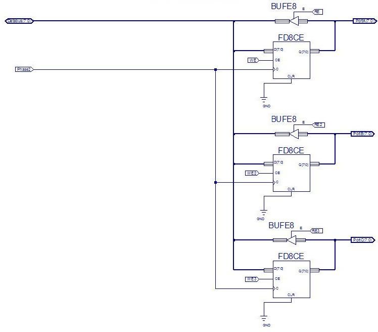
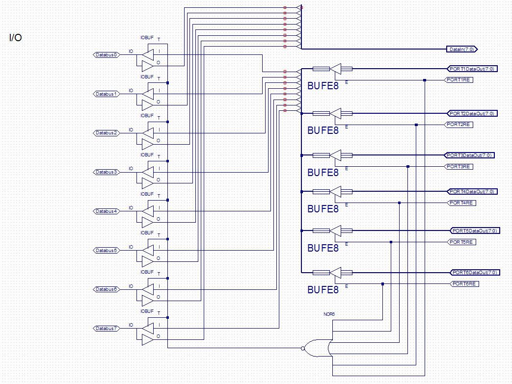
Below is a module similar to one I'm currently using successfully to interface the 6502 databus to multiple, readable output ports inside the FPGA. The only difference is, I've renamed some assignments and added more ports to express the idea more fully.
Databus(7:0) on the left, is assigned to pins on the FPGA. They connect directly to the 6502.
DataIn(7:0) on the top right is common to all the inputs of all the 8-bit PORTs, present inside other modules.
The PORTxRE (read enable) signals from each PORT are NOR'd, to put the data from the corresponding PORT onto the Databus.
I can only speak from my use ot FPGA's and CPLD's using schematic entry as I have not crossed the bridge to HDL yet, but I can say this: That link I had posted has given me insight to problems I've been having.
This what I have learned about implementing bidirectional buses inside CPLD's & FPGA's:
When working with CPLD's, you can have a bidirectional bus that goes to each of your internal ports.
RE, WE are Read Enable & Write Enable signals decoded with Address and R/W.
When working with FPGA's however, you can have only 1 point within the entire IC that is bidirectional (i.e. high impedance "Z" state). So, in that link to the Xilinx forums I mentioned earlier, Gabor stated "... it is best to have this bidirectional entry point at the highest level in your design...".
Below is a module similar to one I'm currently using successfully to interface the 6502 databus to multiple, readable output ports inside the FPGA. The only difference is, I've renamed some assignments and added more ports to express the idea more fully.
Databus(7:0) on the left, is assigned to pins on the FPGA. They connect directly to the 6502.
DataIn(7:0) on the top right is common to all the inputs of all the 8-bit PORTs, present inside other modules.
The PORTxRE (read enable) signals from each PORT are NOR'd, to put the data from the corresponding PORT onto the Databus.
-
ElEctric_EyE
- Posts: 3260
- Joined: 02 Mar 2009
- Location: OH, USA
So now I have a 7-bit (A14-A20) RAMBANK PORT and a 5-bit (A14-A18) ROMBANK PORT that I can perform INC/DEC on. At least I have proven it on the RAMBANK.
The past few days I've been trying to figure out how to INIT an FD8CE for the ROMBANK as it needs to start out with upper bank selected. I need to INIT the 8-bit port for $FF on powerup.
Sounds easy, but I've been having no luck.
Everything else is working.
I know this because when I disconnect the ROMBANK pins (A14-A18 going to the 512Kx8 EEPROM), inside the FPGA, from the PORT and connect each of these pins individually to VCC, the system works.
Can anyone help with Flip Flop INIT values?
ElEctric_EyE wrote:
The past few days I've been trying to figure out how to INIT an FD8CE for the ROMBANK as it needs to start out with upper bank selected. I need to INIT the 8-bit port for $FF on powerup.
Sounds easy, but I've been having no luck.
Sounds easy, but I've been having no luck.
If you don't want to place a ton of FDCPs, there's a simple workaround: place an INV8 directly before and after the FD8CP. The register will then store inverted data, and the powerup value will be $FF instead of $00.
so long,
Hias
-
ElEctric_EyE
- Posts: 3260
- Joined: 02 Mar 2009
- Location: OH, USA
HiassofT wrote:
Having an FD8CP would help a lot (there seems to be only an FDCP in the xilinx library...
I think I may have made abit of progress INIT'ing a FD8CE....
I was right clicking on the FD8CE, which is an 8-bit D Flip Flop w/ clear enable controlling the ROMBANK A14-A18 (using 5 of 8 bits) in my PWA project, and selected "Object Properties". Then chose "NEW", then "Attribute Name": INIT. It then prompts you for a string by default. And I tried many selections, and many value entries. This is what has not worked in ISE 10.1, schematic entry.
I posted on the Xilinx forums a couple days ago and got no response. sniff, sniff, heh.
Probably means my question is self evident, which got me searching the ISE10.1's help index.
...This morning (11/8/10), I actually read the Help, and searched for "Initialize flip flops and latches".
It describes how to initialize flip flops and latches using a constraints file.
I successfully made one this morning, but can't test it till tomorrow!
(11/9/10) Making a constraints file worked! It gives you the choice to assign 1 or 0 to each bit of any flip flop or latch in the design on powerup.
ElEctric_EyE wrote:
HiassofT wrote:
Having an FD8CP would help a lot (there seems to be only an FDCP in the xilinx library...
I also have to say that I haven't used the schematic entry feature yet, I prefer VHDL :-)
Some 5 or 6 years ago I had a similar problem, I wanted to init registers on a Lattice Mach4A5, using ispLever 4 or so, but couldn't get it to work. I'm not sure what went wrong, the datasheet explicitly mentioned asynchronous reset/preset plus powerup logic in the macrocell description. Maybe I did something wrong, maybe ispLever had some bug (I wouldn't rule that out, I already ran into several ispLever oddities before).
So I added a powerup/reset input to my logic and implemented it like this:
Code: Select all
if (powerup == '0') then
    register <= init_value;
else
    if (rising_edge(clk)) then
        register <= databus;
    end if;
end if;so long,
Hias
fachat wrote:
BigDumbDinosaur wrote:
Code: Select all
entity RB65 is
...
Might have been an error in my code though.
Code: Select all
	datain <= data when (phi2 = '1');
	data <= dataout when (phi2 = '1' and Nsel = '0' and rNw = '1')
					else "ZZZZZZZZ";
Maybe just the compiler wasn't intelligent enough on my earlier tries to detect this logic or whatever. I did separate the two internal busses (read bus "datain" and write bus "dataout" this time though)
Thanks Ruud!
André