Stage 2, which I'm working on now, forces all the upper banking addresses low. So I have to temp remove all the opcode detecting hardware (not tested yet). Also, I have abit of reworking to do softwarewise, because the last iteration used an 8K EEPROM for the software, and a separate 512K EEPROM for character fonts, strings, etc.. This version uses 1 512K EEPROM for everything. Not to mention the Display is a little different...
I must say working with FPGA's/CPLD's is very enjoyable and rewarding. All one must have is a general idea of what to accomplish. Heck, looking back, using a 144-pin or 208-pin FPGA would allow you to hook up all the 6502's outputs and inputs, throw in a "few" 2Mx8 SRAM's an EEPROM, and you could have a system you could develop without having to rewire a thing!
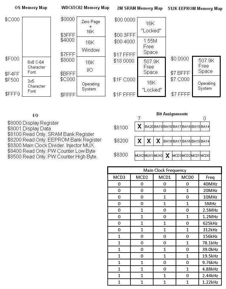
The 2M SRAM address decoding is done in such away that when $0000-$3FFF is on the address bus, the SRAM sees all zero's on A14-A20. When $C000-$FFFF is present, A14-A20 are all one's. The SRAM does not see the SRAM Bank register in these cases. This preserves zero page, and a good chunk of RAM for registers etc., and the OS/interrupt/reset vectors. Here are my memory maps: