Page 2 of 8
Re: From the sublime to the ridiculous - 8-byte PROM
Posted: Wed May 21, 2025 7:56 pm
by barnacle
Aesthetic enough?
I extended it slightly to use the full eurocard; a second card would hold the processor.
Two '138s select one of 16 lines; four '541s and half a '139 choose the desired block. There's no 'chip select'; a single ~rd signal is sufficient.
With 10k pull-up resistors, I calculate a maximum current of 16mA (and an average of half that); speed should be on the order of 150ns. Reducing the resistor value will increase the speed (charging the input capacitance of the '541s faster) but also increase the current consumption.
As drawn, it requires a diode to be inserted where a zero is required in the data byte with the link left open where a one is needed. As an alternative, replace the '541s with '540s (inverting) to get ones where the diode is inserted.
If anyone wants the gerbers, let me know. I probably won't build this, but it would be nice to know if anyone does. The total cost looks affordable: JLC are quoting me ten dollars (plus postage) for five PCBs, and the BOM is around eleven dollars (minimum quantities of five for the chips and the connector, and a thousand diodes - probably enough for four ROMs), again, plus postage.
Neil
Re: From the sublime to the ridiculous - 8-byte PROM
Posted: Wed May 21, 2025 8:06 pm
by barnacle
(It occurs to me that there is half a '139 left over, and some spare input pins: one could supply A6 and A7 and select with a link to create a memory bank with the heady size of 256 bytes!)
Re: From the sublime to the ridiculous - 8-byte PROM
Posted: Wed May 21, 2025 8:52 pm
by GARTHWILSON
A '154 is a step up from the '138 too, a 4-to-16-line decoder. The '251 might be worth looking at too, as an 8-to-1 multiplexer with tri-state outputs. Then, to make it smaller (or put more in the same size), you could put parts on both sides. 
Re: From the sublime to the ridiculous - 8-byte PROM
Posted: Thu May 22, 2025 4:54 am
by barnacle
I always forget about the '154, probably because I found the early dip packages (0.6" 24 pin) so large and didn't tend to use it.
The '251 I'm not so sure about; I think I'd need eight of them (one per bit) so until I get to a 128 byte DROM there's no part advantage.
Double sided... hmm. Not shown on the illustration, but the back of board carries sixteen byte selector signals in rows from top to bottom (where the white lines are as it happens). I suspect it would require a four-layer board to keep things clean...
On the other hand, the question is: is 64 bytes enough, say on a Neolithic-style SBC with a 6850, to allow a terminal to enter code to a fixed memory location, perhaps $200 upwards? I believe so, though I haven't really thought about it. For bonus points, how about something with seven segment displays and a 20-key keypad? Not so sure about that; you'd need sixteen bytes just for the character look-up, but it could be possible.
Neil
Re: From the sublime to the ridiculous - 8-byte PROM
Posted: Thu May 22, 2025 9:44 am
by plasmo
In Muntz65 the ROM code to load program to $300-$3ff with bit-bang serial port is 42 bytes, so I’m sure the code can be shorter with 6850. Maybe 32 bytes? IDK.
Bill
Re: From the sublime to the ridiculous - 8-byte PROM
Posted: Thu May 22, 2025 10:38 am
by BigEd
Re: From the sublime to the ridiculous - 8-byte PROM
Posted: Thu May 22, 2025 1:21 pm
by BruceRMcF
If you have one of those SPI serial flash breakout boards from Adafruit ... I think they have them in 2MB ... and a 6522 + serial shift register SPI interface, and a way to toggle that into the memory map for read only, I wonder whether that would fit a two stage bootloader with the 2nd stage a page written into $FF00-$FFFF. Need to send a $30 and three $00 to read from the beginning of the serial Flash, then the data from that address on up with each SPI transfer until select up.
Needing a call to an SPI routine to send the value in A, with the return value in A. This version uses the fact that the first four bytes, which are not data, get overwritten:
Code: Select all
    ....
    LDY #1
    LDX #$FC
    LDA #$30
-   JSR TXSPI
    STA $FF00,X
    LDA #0
    INX
    BNE -
    DEY
    BPL -
    JMP $FF00
... at about 23 bytes, so with top four bytes for the reset vector, that needs setting up the 6522, selecting the serial flash, and the SPI subroutine to fit into 37 bytes.
Also note that the SPI routine doesn't have to actually be a subroutine, it can be embedded where JSR TXSPI is located, saving four bytes from the call and the RTS.
Re: From the sublime to the ridiculous - 8-byte PROM
Posted: Thu May 22, 2025 1:56 pm
by plasmo
After reset a compact flash disk is pointed to its master boot record so a read command will readout the contents of MBR; this facilitates a small bootstrap code. VGA65 bootstrap from CF disk; the code is 32 bytes and resides in CPLD.
Bill
Re: From the sublime to the ridiculous - 8-byte PROM
Posted: Thu May 22, 2025 2:32 pm
by barnacle
I played around with Garth's suggestion of the '154, and added a block select link.
I think that 64 bytes is as many diodes as can be _conveniently_ placed on one side. Using both sides will definitely require a four layer board - effectively, it's two of these glued back to back, and I think that's getting a little silly

If you want more boot, build up to four of these for

256 bytes!
(which, incidentally, was the total memory of my first computer).
Neil
p.s. my mind has a bad case of the Schmetterlingen. I really must stop chasing these wild ideas

Re: From the sublime to the ridiculous - 8-byte PROM
Posted: Thu May 22, 2025 2:50 pm
by BigDumbDinosaur
Re: From the sublime to the ridiculous - 8-byte PROM
Posted: Thu May 22, 2025 4:45 pm
by BruceRMcF
After reset a compact flash disk is pointed to its master boot record so a read command will readout the contents of MBR; this facilitates a small bootstrap code. VGA65 bootstrap from CF disk; the code is 32 bytes and resides in CPLD.
Bill
Yes, a compact flash is real handy if one has one on hand, but for a cheapskate, there's also an appeal for a $3 2MB SPI Flash breakout board -- though admittedly it does need a 3.3v power supply in addition to VCC, for the voltage converters on the breakout.
Re: From the sublime to the ridiculous - 8-byte PROM
Posted: Fri May 23, 2025 7:19 am
by barnacle
This code looks as if it might work; it expects a binary file of 1k length (or any other number of pages, but hard coded) to load and execute from $200. At 115200 baud, there's 86us per byte available to load and store.
Code: Select all
                        ; minimal initial boot - 64 bytes or fewer
                        ;
                        ; 65c02, 6850
                        ;
                        ; accept bytes from serial port
                        ; expect a binary block 1k in size ($400)
                        ; after this is received, execute from $200

                        ;-----------------------------------------------------
                        ;
                        ; ACIA hardware locations

a001 =                  ACIAData	equ $a001
a000 =                  ACIAStatus	equ $a000

000d =                  CR			equ $0d

                        	bss
0000 =                  	org 0
0000 =                  mem_ptr	ds 2		; and put it [here]

                        	code
ffc0 =                  	org $ffc0

                        	; don't bother with the stack
                        	; decimal mode cleared on reset

ffc0 :                  main:
ffc0 : 6400             	stz mem_ptr
ffc2 : a902             	lda #$02
ffc4 : 8501             	sta mem_ptr+1		; set address pointer
ffc6 : 1a               	inc a
ffc7 : 8d00a0           	sta ACIAStatus		; reset the uart (with $03)
ffca : a995             	lda #$95			; 115k2, 8-n-1, Rx interrupt
                        						; interrupt pin controls CTS; does not interrupt
                        						; the processor
ffcc : 8d00a0           	sta ACIAStatus


                        ;-----------------------------------------------------
                        ; wait until a key is pressed and return it in A
                        ;
ffcf :                  wait_char:
ffcf : ad00a0           	lda ACIAStatus
ffd2 : 6a               	ror a
ffd3 : 90fa             	bcc wait_char		; carry set when new char arrives
ffd5 : ad01a0           	lda ACIAData
ffd8 : 9200             	sta (mem_ptr)		; get the binary byte
ffda : e600             	inc mem_ptr			; save it
ffdc : d0f1             	bne wait_char		; back for more
ffde : e601             	inc mem_ptr+1		; increment page
ffe0 : a501             	lda mem_ptr+1
ffe2 : c906             	cmp #6				; have we received 1k yet?
ffe4 : d0e9             	bne wait_char		; nope...
ffe6 : 4c0002           	jmp $200			; else execute

fffc =                  	org $fffc
fffc : c0ff             	dw	main
It's bigger than the CF 32-byte code because it has to initialise the serial port... 41 bytes. I can't test this on Symon since its emulated 6850 lives in the middle of my rom ($ffd0,1)
I wanted to be able to use a keyboard to send hex characters and execute once the 'x' is seen:
but the code is way too big; even using e.g. @ to O for $0 to $f is a little over the limit. If I want to go that way I'll have to glue some more diodes on the back of the board.
The advantage of the serial port is that it doesn't require a pre-programmed CF card which is easier than programming an EEPROM or EPROM, but still not trivial.
Neil
Re: From the sublime to the ridiculous - 8-byte PROM
Posted: Fri May 23, 2025 2:05 pm
by BruceRMcF
... The advantage of the serial port is that it doesn't require a pre-programmed CF card which is easier than programming an EEPROM or EPROM, but still not trivial. ...
Yes, that's an aspect of the serial port approach that is appealing.
If the widely available SPI NOR Flash programmers based on the CH341A can be made to program the Adafruit SPI flash breakout board, that brings the cost of the programmer down into the $10 range, but of course a simple SPI flash chip has no wear leveling ... an issue the serial port approach completely avoids.
~~~~~~~
The 8x8byte PROM board got me thinking it would be fitting in glue-logic based board, which got me thinking about setting it up to only be visible at /Reset and then it is made to disappear. Say there is a 6522 somewhere that has an available output pin to drive the /SRAM_RD line, which is terminated by a pull up resister.
Then the toggling could be done with a /RD line to the SRAM being held high in the /Reset state and released by pulling /SRAM_RD low, with the /RD line to the Diode board now being held high. I was thinking that could be done with a quad 2-input NAND, which can give an active low trigger SR latch in two NANDs, with the other two NANDs generating the two /RD lines.
In terms of the quad 2NAND in the 74 series, that might be:
Code: Select all
Quad 2NAND
Pin01: 1A   Pin14: VCC
Pin02: 1B   Pin13: 4B
Pin03: 1Y   Pin12: 4A
Pin04: 2A   Pin11: 4Y
Pin05: 2B   Pin10: 3B
Pin06: 2Y   Pin09: 3A
Pin07: GND  Pin08: 3Y

/RD Latch
R/W  Latched      NAND
0      0          => 1
0      1          => 1
1      0          => 1
1      1          => 0

So the /DIODE_RD gate takes its latch input from the /Q output of the latch, which is 1 on reset and 0 after the SR is set, and the /SRAM_RD gate takes its latch input from the Q output of the latch, which is 0 when the latch is reset and 1 after the latch is set.

1A <= /CPU_RESET  "For sanity, /R"
1B <= 4Y
1Y => 4A => 2A    "/Q = /PROM_Latch"

4B <= 6522x0_PB1  "/S"
4A <= 1Y
4Y => 1B => 3B    "Q = PROM_Latch"

2A <= 1Y          "/PROM"
2B <= CPU_R/W
2Y => /SRAM_RD    "/(Read # /PROM_Latch)"

3A <= CPU_R/W
3B <= 4Y          "PROM"
3Y => /DIODE_RD   "/(/Read # PROM_Latch)"
I looked at a system that has two VIA's somewhere above the zero page, using the VIA0 shift register is SPI MOSI under timer 2 control, with the lower latch of T2 set to 1 for a 6 PHI2 serial clock cycle, and CB1 of VIA0 tied to CBA of VIA1 to shift MISO into VIA1 under CB1 control. So store to the VIA0 SR, wait 48 clock cycles, and load from VIA1 SR for a single SPI transfer. There is just exactly enough space to set the hardware stack and set up a loop to load 8KB to $E000-$FFFF from the beginning of an SPI serial Flash.
If CA2 is used as the /SRAM_RD control latch to allow reading from RAM, then the JMP $E000 has to be placed below the six bytes of interrupt/reset vectors in the loaded content, since the JMP will occur after the diode board has been switched out.
Code: Select all
PB = $00
PA = $01
DDRB = $02
DDRA = $03
TCRL = $08
SR = $0A
ACR = $0B
PANI = $0F

SROT2 = %00010100 ; SR shift Out on Timer 2 (lower latch underflow)
SRICB1 = %00011000 ; SR shift In on CB1 (rising pulse)

VIA0 = $0300 ; Hypothetically
VIA1 = $0310 ; Hypothetically

V = $00

* = $FFC0

BOOT:
	LDX #$FF
	TXS
	LDA #1
	STA VIA0+TCRL
	LDA #SROT2
	TSB VIA0+ACR
	LDA #SRICB1
	TSB VIA1+ACR
	LDA #$DF
	STA V+1
	STZ V
	LDY #$FC
	LDA #$30
--	STA VIA0+SR
	LDX #9
-	DEX
	BNE -
	LDA VIA1+SR
	STA (V),Y
	LDA #0
	INY
	BNE --
	INC V+1
	BMI --
	LDA #%00001100
	TSB VIA0+$0C
	JMP $E000
IRQ_VECTORS: ; Must be = $FFFA
	!word 0,BOOT,0
Re: From the sublime to the ridiculous - 8-byte PROM
Posted: Sun May 25, 2025 2:43 am
by Dr Jefyll
I'm late to the party, but maybe now is a good moment to slip in with another sublime/ridiculous case study on the diode ROM theme.
The photos above show a circuit board with a diode array on one side and a DIP switch array on the other. Every diode has a switch in series, and the result could perhaps be called a
PPROM, or
Pencil-Programmable Read Only Memory! (Or, rather than a
pencil, you could use a
prod or other
poking-tool instead.)
I created the board to measure and control the motion of film in a giant camera used in the printing industry. My client wanted the camera to do double exposures (ie, "step and repeat"), and I was hired to retrofit this non-standard feature. (An engineer from the camera's manufacturer had already tried, but failed to achieve the necessary precision because his time delay-based approach relied on repeatable performance from the clutch/brake mechanism used to start and stop the film.)
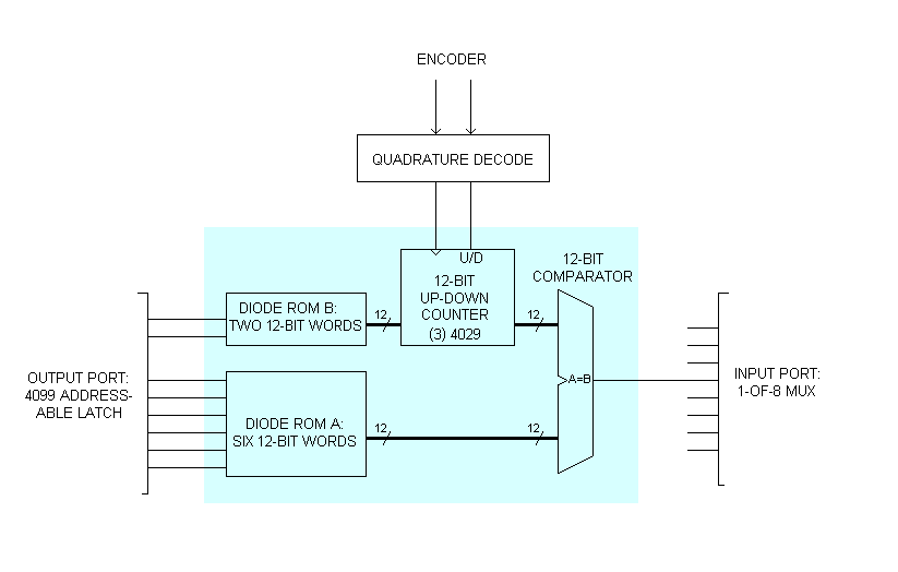
My approach was to start and stop the film according to quadrature pulses from a rotary encoder which I added to the camera's transport mechanism. The block diagram below shows the counting logic, which used 4000 Series CMOS to evaluate 12-bit data words. The 12-bit counting mechanism was separate from the processor that did the actual sequencing of machine operations. The latter (located at the far right of the board) was an original, discrete-logic, 1-bit design running at about 100kHz! Quirky, but it worked. Nowadays I would use a different approach, but in 1981 (?) the available technology was rather limited, and so too was my experience.

There's more on the project
here.
-- Jeff
- Blk_Dgm excerpt.png (6.62 KiB) Viewed 451 times
Re: From the sublime to the ridiculous - 8-byte PROM
Posted: Sun May 25, 2025 7:19 am
by BigEd
Now, that's what I call sublime!